Si5369-EVB Silicon Laboratories Inc, Si5369-EVB Datasheet - Page 26
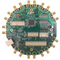
Si5369-EVB
Manufacturer Part Number
Si5369-EVB
Description
MCU, MPU & DSP Development Tools SI5369 DEV KIT
Manufacturer
Silicon Laboratories Inc
Specifications of Si5369-EVB
Processor To Be Evaluated
Si5369
Interface Type
I2C, SPI
Operating Supply Voltage
3.3 V
Lead Free Status / Rohs Status
Details


Reset value = 0100 0010
Reset value = 0000 0101
26
Register 2.
Register 3.
Name
Name
Type
Type
7:4
3:0
7:6
3:0
Bit
Bit
Bit
Bit
5
4
CKSEL_REG [1:0] CKSEL_REG.
BWSEL_REG [3:0]
CKSEL_REG [1:0]
D7
D7
SQ_ICAL
Reserved
DHOLD
Reserved
Name
Name
R/W
BWSEL_REG [3:0]
D6
D6
If the device is operating in manual register-based clock selection mode
(AUTOSEL_REG = 00), and CKSEL_PIN = 0, then these bits select which input
clock will be the active input clock. If CKSEL_PIN = 1, the CKSEL[1:0] input pins
continue to control clock selection and CKSEL_REG is of no consequence.
00: CKIN_1 selected.
01: CKIN_2 selected.
10: CKIN_3 selected.
11: CKIN_4 selected.
DHOLD.
Forces the part into digital hold. This bit overrides all other manual and automatic
clock selection controls.
0: Normal operation.
1: Force digital hold mode. Overrides all other settings and ignores the quality of all
of the input clocks.
SQ_ICAL.
This bit determines if the output clocks will remain enabled or be squelched (dis-
abled) during an internal calibration. See Table 8.
0: Output clocks enabled during ICAL.
1: Output clocks disabled during ICAL.
BWSEL_REG.
Selects nominal f3dB bandwidth for PLL. See the DSPLLsim for settings. After
BWSEL_REG is written with a new value, an ICAL is required for the change to
take effect.
R/W
DHOLD
R/W
D5
D5
Preliminary Rev. 0.4
SQ_ICAL
R/W
D4
D4
Function
D3
D3
Function
D2
D2
Reserved
Reserved
R
R
D1
D1
D0
D0
Related parts for Si5369-EVB
Image
Part Number
Description
Manufacturer
Datasheet
Request
R

Part Number:
Description:
SMD/C°/SINGLE-ENDED OUTPUT SILICON OSCILLATOR
Manufacturer:
Silicon Laboratories Inc
Part Number:
Description:
Manufacturer:
Silicon Laboratories Inc
Datasheet:
Part Number:
Description:
N/A N/A/SI4010 AES KEYFOB DEMO WITH LCD RX
Manufacturer:
Silicon Laboratories Inc
Datasheet:
Part Number:
Description:
N/A N/A/SI4010 SIMPLIFIED KEY FOB DEMO WITH LED RX
Manufacturer:
Silicon Laboratories Inc
Datasheet:
Part Number:
Description:
N/A/-40 TO 85 OC/EZLINK MODULE; F930/4432 HIGH BAND (REV E/B1)
Manufacturer:
Silicon Laboratories Inc
Part Number:
Description:
EZLink Module; F930/4432 Low Band (rev e/B1)
Manufacturer:
Silicon Laboratories Inc
Part Number:
Description:
I°/4460 10 DBM RADIO TEST CARD 434 MHZ
Manufacturer:
Silicon Laboratories Inc
Part Number:
Description:
I°/4461 14 DBM RADIO TEST CARD 868 MHZ
Manufacturer:
Silicon Laboratories Inc
Part Number:
Description:
I°/4463 20 DBM RFSWITCH RADIO TEST CARD 460 MHZ
Manufacturer:
Silicon Laboratories Inc
Part Number:
Description:
I°/4463 20 DBM RADIO TEST CARD 868 MHZ
Manufacturer:
Silicon Laboratories Inc
Part Number:
Description:
I°/4463 27 DBM RADIO TEST CARD 868 MHZ
Manufacturer:
Silicon Laboratories Inc
Part Number:
Description:
I°/4463 SKYWORKS 30 DBM RADIO TEST CARD 915 MHZ
Manufacturer:
Silicon Laboratories Inc
Part Number:
Description:
N/A N/A/-40 TO 85 OC/4463 RFMD 30 DBM RADIO TEST CARD 915 MHZ
Manufacturer:
Silicon Laboratories Inc
Part Number:
Description:
I°/4463 20 DBM RADIO TEST CARD 169 MHZ
Manufacturer:
Silicon Laboratories Inc