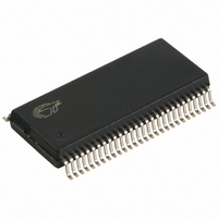
CY7C68001-56PVXC Cypress Semiconductor Corp, CY7C68001-56PVXC Datasheet - Page 30

CY7C68001-56PVXC
Manufacturer Part Number
CY7C68001-56PVXC
Description
IC USB INTERFACE SX2 56-SSOP
Manufacturer
Cypress Semiconductor Corp
Type
USBr
Series
CY7Cr
Datasheet
1.CY7C68001-56PVXC.pdf
(45 pages)
Specifications of CY7C68001-56PVXC
Package / Case
56-SSOP
Protocol
USB 2.0
Voltage - Supply
3 V ~ 3.6 V
Mounting Type
Surface Mount
Maximum Operating Temperature
+ 70 C
Minimum Operating Temperature
0 C
Mounting Style
SMD/SMT
Operating Temperature Range
0 C to + 70 C
Operating Supply Voltage
3.3 V
Core Size
8 Bit
No. Of I/o's
35
Ram Memory Size
256Byte
Embedded Interface Type
SPI, USB
Digital Ic Case Style
SSOP
Supply Voltage Range
3V To 3.6V
Rohs Compliant
Yes
Lead Free Status / RoHS Status
Lead free / RoHS Compliant
Number Of Drivers/receivers
-
Lead Free Status / Rohs Status
Lead free / RoHS Compliant
Other names
428-1864
CY7C68001-56PVXC
CY7C68001-56PVXC
Available stocks
Company
Part Number
Manufacturer
Quantity
Price
Company:
Part Number:
CY7C68001-56PVXC
Manufacturer:
CY
Quantity:
101
Company:
Part Number:
CY7C68001-56PVXC
Manufacturer:
CYPRESS
Quantity:
7
Part Number:
CY7C68001-56PVXC
Manufacturer:
CYPRESS/赛普拉斯
Quantity:
20 000
Figure 13-8.
number of bytes in the FIFO reaches X (value set in AUTOINLEN register) and the second one byte/word short packet being committed
manually using PKTEND. Note that there is at least one IFCLK cycle timing between the assertion of PKTEND and clocking of the
last byte of the previous packet (causing the packet to be committed automatically). Failing to adhere to this timing, results in the FX2
failing to send the one byte/word short packet.
Table 13-13. Slave FIFO Synchronous Address Parameters
Document #: 38-08013 Rev. *J
t
t
t
IFCLK
SFA
FAH
PKTEND
FIFOADR
DATA
IFCLK
SLWR
Parameter
shows a scenario where two packets are being committed. The first packet gets committed automatically when the
Interface Clock Period
FIFOADR[2:0] to Clock Setup Time
Clock to FIFOADR[2:0] Hold Time
SLCS#/FIFOADR[2:0]
Figure 13-8. Slave FIFO Synchronous Write Sequence and Timing Diagram
t
SFA
t
IFCLK
Figure 13-9. Slave FIFO Synchronous Address Timing Diagram
>= t
t
SFD
IFCLK
SWR
X-4
t
FDH
Description
t
SFD
X-3
t
FDH
t
SFD
X-2
[14]
t
FDH
t
SFA
t
SFD
t
FAH
X-1
t
FDH
Min
20
25
10
t
SFD
X
t
FDH
At least one IFCLK cycle
Max
200
t
SFD
1
>= t
t
FDH
WRH
CY7C68001
t
t
FAH
SPE
Unit
ns
ns
ns
Page 30 of 45
t
PEH
[+] Feedback


