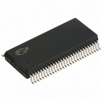
CY7C68001-56PVXC Cypress Semiconductor Corp, CY7C68001-56PVXC Datasheet - Page 10

CY7C68001-56PVXC
Manufacturer Part Number
CY7C68001-56PVXC
Description
IC USB INTERFACE SX2 56-SSOP
Manufacturer
Cypress Semiconductor Corp
Type
USBr
Series
CY7Cr
Datasheet
1.CY7C68001-56PVXC.pdf
(45 pages)
Specifications of CY7C68001-56PVXC
Package / Case
56-SSOP
Protocol
USB 2.0
Voltage - Supply
3 V ~ 3.6 V
Mounting Type
Surface Mount
Maximum Operating Temperature
+ 70 C
Minimum Operating Temperature
0 C
Mounting Style
SMD/SMT
Operating Temperature Range
0 C to + 70 C
Operating Supply Voltage
3.3 V
Core Size
8 Bit
No. Of I/o's
35
Ram Memory Size
256Byte
Embedded Interface Type
SPI, USB
Digital Ic Case Style
SSOP
Supply Voltage Range
3V To 3.6V
Rohs Compliant
Yes
Lead Free Status / RoHS Status
Lead free / RoHS Compliant
Number Of Drivers/receivers
-
Lead Free Status / Rohs Status
Lead free / RoHS Compliant
Other names
428-1864
CY7C68001-56PVXC
CY7C68001-56PVXC
Available stocks
Company
Part Number
Manufacturer
Quantity
Price
Company:
Part Number:
CY7C68001-56PVXC
Manufacturer:
CY
Quantity:
101
Company:
Part Number:
CY7C68001-56PVXC
Manufacturer:
CYPRESS
Quantity:
7
Part Number:
CY7C68001-56PVXC
Manufacturer:
CYPRESS/赛普拉斯
Quantity:
20 000
A two-step process is employed to clear an endpoint data toggle
bit to 0. First, write to the TOGCTL register with an endpoint
address (EP3:EP0) plus a direction bit (IO). Keeping the
endpoint and direction bits the same, write a “1” to the R (reset)
bit. For example, to clear the data toggle for EP6 configured as
an “IN” endpoint, write the following values sequentially to
TOGCTL:
00010110b
00110110b
Following is the sequence of events that the master should
perform to set this register to 0x16:
■
■
Document #: 38-08013 Rev. *J
Send Low Byte of the Register (0x83)
❐
❐
❐
Send High Byte of the Register (0xE6)
❐
❐
❐
Command address write of address 0x3A
Command data write of upper nibble of the Low Byte of Reg-
ister Address (0x08)
Command data write of lower nibble of the Low Byte of Reg-
ister Address (0x03)
Command address write of address 0x3B
Command data write of upper nibble of the High Byte of
Register Address (0x0E)
Command data write of lower nibble of the High Byte of Reg-
ister Address (0x06)
■
The same command sequence needs to be followed to set
TOGCTL register to 0x36. The same command protocol
sequence can be used to reset the data toggle for the other
endpoints.
In order to read the status of this register, the external master
must do the following sequence of events:
■
■
■
Send the actual value to write to the register Register (in this
case 0x16)
❐
❐
❐
Send Low Byte of the Register (0x83)
❐
❐
❐
Send High Byte of the Register (0xE6)
❐
❐
❐
Get the actual value from the TOGCTL register (0x16)
❐
Command address write of address0x3C
Command data write of upper nibble of the register value
(0x01)
Command data write of lower nibble of the register value
(0x06)
Command address write of 0x3A
Command data write of upper nibble of the Low Byte of Reg-
ister Address (0x08)
Command data write of lower nibble of the Low Byte of Reg-
ister Address (0x03)
Command address write of address 0x3B
Command data write of upper nibble of the High Byte of
Register Address (0x0E)
Command data write of lower nibble of the High Byte of Reg-
ister Address (0x06)
Command address READ of 0x3C
CY7C68001
Page 10 of 45
[+] Feedback


