CY7C68001-56PVXC Cypress Semiconductor Corp, CY7C68001-56PVXC Datasheet - Page 3
CY7C68001-56PVXC
Manufacturer Part Number
CY7C68001-56PVXC
Description
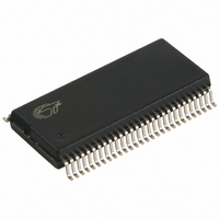
IC USB INTERFACE SX2 56-SSOP
Manufacturer
Cypress Semiconductor Corp
Type
USBr
Series
CY7Cr
Datasheet
1.CY7C68001-56PVXC.pdf
(45 pages)
Specifications of CY7C68001-56PVXC
Package / Case
56-SSOP
Protocol
USB 2.0
Voltage - Supply
3 V ~ 3.6 V
Mounting Type
Surface Mount
Maximum Operating Temperature
+ 70 C
Minimum Operating Temperature
0 C
Mounting Style
SMD/SMT
Operating Temperature Range
0 C to + 70 C
Operating Supply Voltage
3.3 V
Core Size
8 Bit
No. Of I/o's
35
Ram Memory Size
256Byte
Embedded Interface Type
SPI, USB
Digital Ic Case Style
SSOP
Supply Voltage Range
3V To 3.6V
Rohs Compliant
Yes
Lead Free Status / RoHS Status
Lead free / RoHS Compliant
Number Of Drivers/receivers
-
Lead Free Status / Rohs Status
Lead free / RoHS Compliant
Other names
428-1864
CY7C68001-56PVXC
CY7C68001-56PVXC
Available stocks
Company
Part Number
Manufacturer
Quantity
Price
Company:

Part Number:
CY7C68001-56PVXC
Manufacturer:
CY
Quantity:
101
Company:
Part Number:
CY7C68001-56PVXC
Manufacturer:
CYPRESS
Quantity:
7
Part Number:
CY7C68001-56PVXC
Manufacturer:
CYPRESS/赛普拉斯
Quantity:
20 000


■
■
■
■
■
5.3.2 Default Enumeration
An optional default descriptor can be used to simplify enumer-
ation. Only the Vendor ID (VID), Product ID (PID), and Device ID
(DID) need to be loaded by the SX2 for it to enumerate with this
default setup. This information is either loaded from an EEPROM
in the case when the presence of an EEPROM
detected, or the external master may simply load a VID, PID, and
DID when no EEPROM is present. In this default enumeration,
the SX2 uses the in-built default descriptor (refer to
Descriptor
If the descriptor length loaded from the EEPROM is 6, SX2 loads
a VID, PID, and DID from the EEPROM and enumerate. The
VID, PID, and DID are loaded LSB, then MSB. For example, if
the VID, PID, and DID are 0x0547, 0x1002, and 0x0001, respec-
tively, then the bytes should be stored as:
■
If there is no EEPROM, SX2 waits for the external master to
provide the descriptor information. To use the default descriptor,
the external master must write to the appropriate register (0x30)
with descriptor length equal to 6 followed by the VID, PID, and
DID. Refer to
mation on how the external master may load the values.
The default descriptor enumerates the following endpoints:
Document #: 38-08013 Rev. *J
IFCONFIG: The IFCONFIG byte contains the settings for the
IFCONFIG register. The IFCONFIG register bits are defined in
IFCONFIG Register 0x01
requires an interface configuration different from the default,
that interface can be specified by this byte.
POLAR: The Polar byte contains the polarity of the FIFO flag
pin signals. The POLAR register bits are defined in
Register 0x04
polarity different from the default, the polarity can be specified
by this byte.
Descriptor: The Descriptor byte determines if the SX2 loads
the descriptor from the EEPROM. If this byte = 0xC4, the SX2
loads the descriptor starting with the next byte. If this byte does
not equal 0xC4, the SX2 waits for descriptor information from
the external master.
Descriptor Length: The Descriptor length is within the next
two bytes and indicate the length of the descriptor contained
within the EEPROM. The length is loaded least significant byte
(LSB) first, then most significant byte (MSB).
Byte Index 6 Starts Descriptor Information: The descriptor
can be a maximum of 500 bytes.
0x47, 0x05, 0x02, 0x10, 0x01, 0x00.
on page 37).
Default Enumeration
on page 18. If the external master requires signal
on page 17. If the external master
on page 8 for further infor-
(Table
POLAR
Default
5-1) is
■
■
■
■
The entire default descriptor is listed in
page 37 of this data sheet.
5.4 Interrupt System
5.4.1 Architecture
The SX2 provides an output signal that indicates to the external
master that the SX2 has an interrupt condition, or that the data
from a register read request is available. The SX2 has six
interrupt sources: SETUP, EP0BUF, FLAGS, ENUMOK,
BUSACTIVITY, and READY. Each interrupt can be enabled or
disabled by setting or clearing the corresponding bit in the
INTENABLE register.
When an interrupt occurs, the INT# pin is asserted, and the
corresponding bit is set in the Interrupt Status Byte. The external
master reads the Interrupt Status Byte by strobing SLRD/SLOE.
This presents the Interrupt Status Byte on the lower portion of the
data bus (FD[7:0]). Reading the Interrupt Status Byte automati-
cally clears the interrupt. Only one interrupt request occurs at a
time; the SX2 buffers multiple pending interrupts.
If the external master has initiated a register read request, the
SX2 buffers interrupts until the external master has read the
data. This insures that after a read sequence has begun, the next
interrupt that is received from the SX2 indicates that the corre-
sponding data is available. Following is a description of this
INTENABLE register.
5.4.2 INTENABLE Register Bit Definition
Bit 7: SETUP
If this interrupt is enabled, and the SX2 receives a setup packet
from the USB host, the SX2 asserts the INT# pin and sets bit 7
in the Interrupt Status Byte. This interrupt only occurs if the setup
request is not one that the SX2 automatically handles. For
complete details on how to handle the SETUP interrupt, refer to
Endpoint 0
Endpoint 2: Bulk out, 512 bytes in high speed mode, 64 bytes
in full speed mode
Endpoint 4: Bulk out, 512 bytes in high speed mode, 64 bytes
in full speed mode
Endpoint 6: Bulk in, 512 bytes in high speed mode, 64 bytes in
full speed mode
Endpoint 8: Bulk in, 512 bytes in high speed mode, 64 bytes in
full speed mode.
on page 8 of this data sheet.
Default Descriptor
CY7C68001
Page 3 of 45
on
[+] Feedback
Related parts for CY7C68001-56PVXC
Image
Part Number
Description
Manufacturer
Datasheet
Request
R

Part Number:
Description:
Manufacturer:
Cypress Semiconductor Corp
Datasheet:

Part Number:
Description:
Manufacturer:
Cypress Semiconductor Corp
Datasheet:

Part Number:
Description:
CY7C68001-56PVXCT
Manufacturer:
Cypress Semiconductor Corp
Datasheet:
Part Number:
Description:
IC,Bus Controller,LLCC,56PIN
Manufacturer:
Cypress Semiconductor Corp
Datasheet:

Part Number:
Description:
IC USB EZ-USB SX2 HS 56VQFN
Manufacturer:
Cypress Semiconductor Corp
Datasheet:
Part Number:
Description:
Manufacturer:
Cypress Semiconductor Corp
Datasheet:
Part Number:
Description:
Manufacturer:
Cypress Semiconductor Corp
Datasheet:
Part Number:
Description:
Manufacturer:
Cypress Semiconductor Corp
Datasheet: