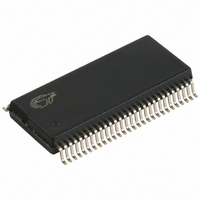
CY7C68001-56PVXC Cypress Semiconductor Corp, CY7C68001-56PVXC Datasheet - Page 17

CY7C68001-56PVXC
Manufacturer Part Number
CY7C68001-56PVXC
Description
IC USB INTERFACE SX2 56-SSOP
Manufacturer
Cypress Semiconductor Corp
Type
USBr
Series
CY7Cr
Datasheet
1.CY7C68001-56PVXC.pdf
(45 pages)
Specifications of CY7C68001-56PVXC
Package / Case
56-SSOP
Protocol
USB 2.0
Voltage - Supply
3 V ~ 3.6 V
Mounting Type
Surface Mount
Maximum Operating Temperature
+ 70 C
Minimum Operating Temperature
0 C
Mounting Style
SMD/SMT
Operating Temperature Range
0 C to + 70 C
Operating Supply Voltage
3.3 V
Core Size
8 Bit
No. Of I/o's
35
Ram Memory Size
256Byte
Embedded Interface Type
SPI, USB
Digital Ic Case Style
SSOP
Supply Voltage Range
3V To 3.6V
Rohs Compliant
Yes
Lead Free Status / RoHS Status
Lead free / RoHS Compliant
Number Of Drivers/receivers
-
Lead Free Status / Rohs Status
Lead free / RoHS Compliant
Other names
428-1864
CY7C68001-56PVXC
CY7C68001-56PVXC
Available stocks
Company
Part Number
Manufacturer
Quantity
Price
Company:
Part Number:
CY7C68001-56PVXC
Manufacturer:
CY
Quantity:
101
Company:
Part Number:
CY7C68001-56PVXC
Manufacturer:
CYPRESS
Quantity:
7
Part Number:
CY7C68001-56PVXC
Manufacturer:
CYPRESS/赛普拉斯
Quantity:
20 000
9.1 IFCONFIG Register 0x01
9.1.1 Bit 7: IFCLKSRC
This bit selects the clock source for the FIFOs. If IFCLKSRC = 0,
the external clock on the IFCLK pin is selected. If IFCLKSRC = 1
(default), an internal 30 or 48 MHz clock is used.
9.1.2 Bit 6: 3048 MHZ
This bit selects the internal FIFO clock frequency. If
3048 MHZ = 0, the internal clock frequency is 30 MHz. If
3048 MHZ = 1 (default), the internal clock frequency is 48 MHz.
9.1.3 Bit 5: IFCLKOE
This bit selects if the IFCLK pin is driven. If IFCLKOE = 0
(default), the IFCLK pin is floated. If IFCLKOE = 1, the IFCLK pin
is driven.
9.1.4 Bit 4: IFCLKPOL
This bit controls the polarity of the IFCLK signal.
■
■
9.1.5 Bit 3: ASYNC
This bit controls whether the FIFO interface is synchronous or
asynchronous. When ASYNC = 0, the FIFOs operate synchro-
nously. In synchronous mode, a clock is supplied either internally
9.2 FLAGSAB/FLAGSCD Registers 0x02/0x03
The SX2 has four FIFO flags output pins: FLAGA, FLAGB, FLAGC, FLAGD.
Document #: 38-08013 Rev. *J
IFCONFIG
Bit #
Bit Name
Read/Write
Default
FLAGSAB
Bit #
Bit Name
Read/Write
Default
FLAGSCD
Bit #
Bit Name
Read/Write
Default
When IFCLKPOL=0, the clock has the polarity shown in all the
timing diagrams in this data sheet (rising edge is the activating
edge).
When IFCLKPOL=1, the clock is inverted (in some cases may
help with satisfying data setup times).
IFCLKSRC
FLAGD3
FLAGB3
R/W
R/W
R/W
7
1
7
0
7
0
3048 MHZ
FLAGB2
FLAGD2
R/W
R/W
R/W
6
1
6
0
6
0
IFCLKOE
FLAGB1
FLAGD1
R/W
R/W
R/W
5
0
5
0
5
0
IFCLKPOL
FLAGD0
FLAGB0
R/W
R/W
R/W
4
0
4
0
4
0
or externally on the IFCLK pin, and the FIFO control signals
function as read and write enable signals for the clock signal.
When ASYNC = 1 (default), the FIFOs operate asynchronously.
No clock signal input to IFCLK is required, and the FIFO control
signals function directly as read and write strobes.
9.1.6 Bit 2: STANDBY
This bit instructs the SX2 to enter a low power mode. When
STANDBY=1, the SX2 enters a low power mode by turning off its
oscillator. The external master should write this bit after it
receives a bus activity interrupt (indicating that the host has
signaled a USB suspend condition). If SX2 is disconnected from
the USB bus, the external master can write this bit at any time to
save power. Once suspended, the SX2 is awakened either by
resumption of USB bus activity or by assertion of its WAKEUP
pin.
9.1.7 Bit 1: FLAGD/CS#
This bit controls the function of the FLAGD/CS# pin. When
FLAGD/CS# = 0 (default), the pin operates as a slave chip select.
If FLAGD/CS# = 1, the pin operates as FLAGD.
9.1.8 Bit 0: DISCON
This bit controls whether the internal pull up resistor connected
to D+ is pulled high or floating. When DISCON = 1 (default), the
pull up resistor is floating simulating a USB unplug. When
DISCON=0, the pull up resistor is pulled high signaling a USB
connection.
FLAGA3
FLAGC3
ASYNC
R/W
R/W
R/W
3
1
3
0
3
0
STANDBY
FLAGC2
FLAGA2
R/W
R/W
R/W
2
0
2
0
2
0
FLAGD/CS#
FLAGA1
FLAGC1
R/W
R/W
R/W
1
0
1
0
1
0
CY7C68001
FLAGC0
FLAGA0
Page 17 of 45
DISCON
R/W
R/W
0
0
0
0
R/W
0
1
0x02
0x03
0x01
[+] Feedback


