CY7C68001-56PVXC Cypress Semiconductor Corp, CY7C68001-56PVXC Datasheet - Page 29
CY7C68001-56PVXC
Manufacturer Part Number
CY7C68001-56PVXC
Description
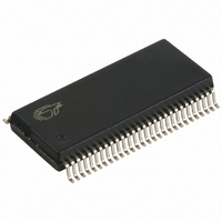
IC USB INTERFACE SX2 56-SSOP
Manufacturer
Cypress Semiconductor Corp
Type
USBr
Series
CY7Cr
Datasheet
1.CY7C68001-56PVXC.pdf
(45 pages)
Specifications of CY7C68001-56PVXC
Package / Case
56-SSOP
Protocol
USB 2.0
Voltage - Supply
3 V ~ 3.6 V
Mounting Type
Surface Mount
Maximum Operating Temperature
+ 70 C
Minimum Operating Temperature
0 C
Mounting Style
SMD/SMT
Operating Temperature Range
0 C to + 70 C
Operating Supply Voltage
3.3 V
Core Size
8 Bit
No. Of I/o's
35
Ram Memory Size
256Byte
Embedded Interface Type
SPI, USB
Digital Ic Case Style
SSOP
Supply Voltage Range
3V To 3.6V
Rohs Compliant
Yes
Lead Free Status / RoHS Status
Lead free / RoHS Compliant
Number Of Drivers/receivers
-
Lead Free Status / Rohs Status
Lead free / RoHS Compliant
Other names
428-1864
CY7C68001-56PVXC
CY7C68001-56PVXC
Available stocks
Company
Part Number
Manufacturer
Quantity
Price
Company:

Part Number:
CY7C68001-56PVXC
Manufacturer:
CY
Quantity:
101
Company:
Part Number:
CY7C68001-56PVXC
Manufacturer:
CYPRESS
Quantity:
7
Part Number:
CY7C68001-56PVXC
Manufacturer:
CYPRESS/赛普拉斯
Quantity:
20 000


Table 13-10. Slave FIFO Synchronous Write Parameters with Externally Sourced IFCLK
Table 13-11. Slave FIFO Synchronous Packet End Strobe Parameters, Internally Sourced IFCLK
Table 13-12. Slave FIFO Synchronous Packet End Strobe Parameters, Externally Sourced IFCLK
There is no specific timing requirement that needs to be met for
asserting PKTEND pin with regards to asserting SLWR.
PKTEND can be asserted with the last data value clocked into
the FIFOs or thereafter. The only consideration is the setup time
t
Although there are no specific timing requirement for the
PKTEND assertion, there is a specific corner case condition that
needs attention while using the PKTEND to commit a one
byte/word packet. There is an additional timing requirement that
need to be met when the FIFO is configured to operate in auto
Document #: 38-08013 Rev. *J
t
t
t
t
t
t
t
t
t
t
t
t
t
t
SPE
IFCLK
SWR
WRH
SFD
FDH
XFLG
IFCLK
SPE
PEH
XFLG
IFCLK
SPE
PEH
XFLG
and the hold time t
Parameter
Parameter
Parameter
IFCLK Period
SLWR to Clock Setup Time
Clock to SLWR Hold Time
FIFO Data to Clock Setup Time
Clock to FIFO Data Hold Time
Clock to FLAGS Output Propagation Time
IFCLK Period
PKTEND to Clock Setup Time
Clock to PKTEND Hold Time
Clock to FLAGS Output Propagation Delay
IFCLK Period
PKTEND to Clock Setup Time
Clock to PKTEND Hold Time
Clock to FLAGS Output Propagation Delay
PEH
Figure 13-7. Slave FIFO Synchronous Packet End Strobe Timing Diagram
must be met.
PKTEND
FLAGS
IFCLK
Description
Description
Description
t
SPE
mode and it is desired to send two packets back to back: a full
packet (full defined as the number of bytes in the FIFO meeting
the level set in AUTOINLEN register) committed automatically
followed by a short one byte/word packet committed manually
using the PKTEND pin. In this particular scenario, user must
make sure to assert PKTEND at least one clock cycle after the
rising edge that caused the last byte/word to be clocked into the
previous auto committed packet.
is the value the AUTOINLEN register is set to when the IN
endpoint is configured to be in auto mode.
t
PEH
t
XFLG
20.83
12.1
14.6
Min
Min
Min
3.6
3.2
4.5
8.6
2.5
20
20
0
[14]
Max
13.5
Max
Max
13.5
200
9.5
Figure
[14]
[14]
[13]
shows this scenario. X
CY7C68001
Unit
Unit
Unit
ns
ns
ns
ns
ns
ns
ns
ns
ns
ns
ns
ns
ns
ns
Page 29 of 45
[+] Feedback
Related parts for CY7C68001-56PVXC
Image
Part Number
Description
Manufacturer
Datasheet
Request
R

Part Number:
Description:
Manufacturer:
Cypress Semiconductor Corp
Datasheet:

Part Number:
Description:
Manufacturer:
Cypress Semiconductor Corp
Datasheet:

Part Number:
Description:
CY7C68001-56PVXCT
Manufacturer:
Cypress Semiconductor Corp
Datasheet:
Part Number:
Description:
IC,Bus Controller,LLCC,56PIN
Manufacturer:
Cypress Semiconductor Corp
Datasheet:

Part Number:
Description:
IC USB EZ-USB SX2 HS 56VQFN
Manufacturer:
Cypress Semiconductor Corp
Datasheet:
Part Number:
Description:
Manufacturer:
Cypress Semiconductor Corp
Datasheet:
Part Number:
Description:
Manufacturer:
Cypress Semiconductor Corp
Datasheet:
Part Number:
Description:
Manufacturer:
Cypress Semiconductor Corp
Datasheet: