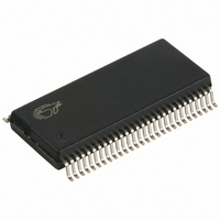
CY7C68001-56PVXC Cypress Semiconductor Corp, CY7C68001-56PVXC Datasheet - Page 23

CY7C68001-56PVXC
Manufacturer Part Number
CY7C68001-56PVXC
Description
IC USB INTERFACE SX2 56-SSOP
Manufacturer
Cypress Semiconductor Corp
Type
USBr
Series
CY7Cr
Datasheet
1.CY7C68001-56PVXC.pdf
(45 pages)
Specifications of CY7C68001-56PVXC
Package / Case
56-SSOP
Protocol
USB 2.0
Voltage - Supply
3 V ~ 3.6 V
Mounting Type
Surface Mount
Maximum Operating Temperature
+ 70 C
Minimum Operating Temperature
0 C
Mounting Style
SMD/SMT
Operating Temperature Range
0 C to + 70 C
Operating Supply Voltage
3.3 V
Core Size
8 Bit
No. Of I/o's
35
Ram Memory Size
256Byte
Embedded Interface Type
SPI, USB
Digital Ic Case Style
SSOP
Supply Voltage Range
3V To 3.6V
Rohs Compliant
Yes
Lead Free Status / RoHS Status
Lead free / RoHS Compliant
Number Of Drivers/receivers
-
Lead Free Status / Rohs Status
Lead free / RoHS Compliant
Other names
428-1864
CY7C68001-56PVXC
CY7C68001-56PVXC
Available stocks
Company
Part Number
Manufacturer
Quantity
Price
Company:
Part Number:
CY7C68001-56PVXC
Manufacturer:
CY
Quantity:
101
Company:
Part Number:
CY7C68001-56PVXC
Manufacturer:
CYPRESS
Quantity:
7
Part Number:
CY7C68001-56PVXC
Manufacturer:
CYPRESS/赛普拉斯
Quantity:
20 000
9.14 INTENABLE Register 0x2E
This register is used to enable/disable the various interrupt
sources, and by default all interrupts are enabled.
9.14.1 SETUP Bit 7
Setting this bit to a 1 enables an interrupt when a setup packet
is received from the USB host.
9.14.2 EP0BUF Bit 6
Setting this bit to a 1 enables an interrupt when the Endpoint 0
buffer becomes available.
9.14.3 FLAGS Bit 5
Setting this bit to a 1 enables an interrupt when an OUT endpoint
FIFO’s state transitions from empty to not-empty.
9.14.4 ENUMOK Bit 2
Setting this bit to a 1 enables an interrupt when SX2 enumeration
is complete.
9.14.5 BUSACTIVITY Bit 1
Setting this bit to a 1 enables an interrupt when the SX2 detects
an absence or presence of bus activity.
Document #: 38-08013 Rev. *J
INTENABLE
Bit #
Bit Name
Read/Write
Default
SETUP EP0
R/W
7
1
BUF
R/W
6
1
FLAGS
R/W
5
1
R/W R/W
4
1
1
3
1
1
ENUM
R/W
OK
2
1
ACTIVITY
BUS
R/W
1
1
READY
R/W
0x2E
0
1
9.14.6 READY Bit 0
Setting this bit to a 1 enables an interrupt when the SX2 has
powered on and performed an internal self-test.
9.15 DESC Register 0x30
This register address is used to write the 500-byte descriptor
RAM. The external master writes two bytes (four command data
transfers) to this address corresponding to the length of the
descriptor or VID/PID/DID data to be written. The external
master then consecutively writes that number of bytes into the
descriptor RAM in nibble format. For complete details, refer to
Enumeration
9.16 EP0BUF Register 0x31
This register address is used to access the 64-byte Endpoint 0
buffer. The external master can read or write to this register to
complete Endpoint 0 data transfers. For complete details, refer
to
9.17 SETUP Register 0x32
This register address is used to access the 8-byte setup packet
received from the USB host. If the external master writes to this
register, it can stall Endpoint 0. For complete details, refer to
Endpoint 0
9.18 EP0BC Register 0x33
This register address is used to access the byte count of
Endpoint 0. For Endpoint 0 OUT transfers, the external master
can read this register to get the number of bytes transferred from
the USB host. For Endpoint 0 IN transfers, the external master
writes the number of bytes in the Endpoint 0 buffer to transfer the
bytes to the USB host. For complete details, refer to
on page 8.
Endpoint 0
on page 8.
on page 8.
on page 8.
CY7C68001
Page 23 of 45
Endpoint 0
[+] Feedback


