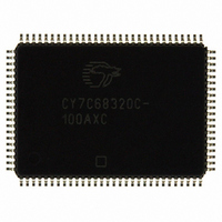
CY7C68320C-100AXC Cypress Semiconductor Corp, CY7C68320C-100AXC Datasheet - Page 16

CY7C68320C-100AXC
Manufacturer Part Number
CY7C68320C-100AXC
Description
IC USB 2.0 BRIDGE AT2LP 100LQFP
Manufacturer
Cypress Semiconductor Corp
Series
EZ-USB AT2LP™r
Type
USB to ATA Bridger
Datasheet
1.CY7C68300C-56PVXC.pdf
(42 pages)
Specifications of CY7C68320C-100AXC
Package / Case
100-LQFP
Controller Type
USB 2.0 Controller
Interface
I²C
Voltage - Supply
3 V ~ 3.6 V
Current - Supply
50mA
Operating Temperature
0°C ~ 70°C
Mounting Type
Surface Mount
Operating Supply Voltage
3.3 V
Supply Current
50 mA
Maximum Operating Temperature
+ 70 C
Minimum Operating Temperature
0 C
Mounting Style
SMD/SMT
Lead Free Status / RoHS Status
Lead free / RoHS Compliant
For Use With
CY4615B - KIT USB TO ATA REFERENCE DESIGN
Lead Free Status / Rohs Status
Lead free / RoHS Compliant
Other names
428-2267
CY7C68320C-100AXC
CY7C68320C-100AXC
Available stocks
Company
Part Number
Manufacturer
Quantity
Price
Company:
Part Number:
CY7C68320C-100AXC
Manufacturer:
Cypress
Quantity:
151
Company:
Part Number:
CY7C68320C-100AXC
Manufacturer:
Cypress Semiconductor Corp
Quantity:
10 000
Table 6. ATACB Field Descriptions
Document 001-05809 Rev. *B
Byte
0
1
2
bVSCBSignature
bVSCBSubCommand
bmATACBActionSelect
Field Name
This field indicates to the CY7C68300C/CY7C68301C that the ATACB
contains a vendor-specific command block. This value of this field must match
the value in EEPROM address 0x04 for the command to be recognized as a
vendor-specific ATACB command.
This field must be set to 0x24 for ATACB commands.
This field controls the execution of the ATACB according to the bitfield values:
Bit 7 IdentifyPacketDevice – This bit indicates that the data phase of the
command contains ATAPI (0xA1) or ATA (0xEC) IDENTIFY device data.
Setting IdentifyPacketDevice when the data phase does not contain IDENTIFY
device data results in unspecified device behavior.
0 = Data phase does not contain IDENTIFY device data
1 = Data phase contains ATAPI or ATA IDENTIFY device data
Bit 6 UDMACommand – This bit enables supported UDMA device transfers.
Setting this bit when a non-UDMA capable device is attached results in
undetermined behavior.
0 = Do not use UDMA device transfers (only use PIO mode)
1 = Use UDMA device transfers
Bit 5 DEVOverride – This bit determines whether the DEV bit value is taken
from the value assigned to the LUN during startup or from the ATACB.
0 = The DEV bit is taken from the value assigned to the LUN during startup
1 = The DEV bit is taken from the ATACB field 0x0B, bit 4
Bit 4 DErrorOverride – This bit controls the device error override feature. This
bit must not be set during a bmATACBActionSelect TaskFileRead.
0 = Data accesses are halted if a device error is detected
1 = Data accesses are not halted if a device error is detected
Bit 3 PErrorOverride – This bit controls the phase error override feature. This
bit must not be set during a bmATACBActionSelect TaskFileRead.
0 = Data accesses are halted if a phase error is detected
1 = Data accesses are not halted if a phase error is detected
Bit 2 PollAltStatOverride – This bit determines whether or not the Alternate
Status register is polled and the BSY bit is used to qualify the ATACB operation.
0 = The AltStat register is polled until BSY=0 before proceeding with the ATACB
operation
1 = The ATACB operation is executed without polling the AltStat register.
Bit 1 DeviceSelectionOverride – This bit determines when the device selection
is performed in relation to the command register write accesses.
0 = Device selection is performed before command register write accesses
1 = Device selection is performed following command register write accesses
Bit 0 TaskFileRead – This bit determines whether or not the taskfile register
data selected in bmATACBRegisterSelect is returned. If this bit is set, the
dCBWDataTransferLength field must be set to 8.
0 = Execute ATACB command and data transfer (if any)
1 = Only read taskfile registers selected in bmATACBRegisterSelect and return
0x00h for all others. The format of the 8 bytes of returned data is as follows:
❐
❐
❐
❐
❐
❐
❐
❐
Address offset 0x00 (0x3F6) – Alternate Status
Address offset 0x01 (0x1F1) – Features/Error
Address offset 0x02 (0x1F2) – Sector Count
Address offset 0x03 (0x1F3) – Sector Number
Address offset 0x04 (0x1F4) – Cylinder Low
Address offset 0x05 (0x1F5) – Cylinder High
Address offset 0x06 (0x1F6) – Device/Head
Address offset 0x07 (0x1F7) – Command/Status
Field Description
CY7C68300C, CY7C68301C
CY7C68320C, CY7C68321C
Page 16 of 42
[+] Feedback


