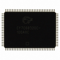
CY7C68320C-100AXC Cypress Semiconductor Corp, CY7C68320C-100AXC Datasheet - Page 12

CY7C68320C-100AXC
Manufacturer Part Number
CY7C68320C-100AXC
Description
IC USB 2.0 BRIDGE AT2LP 100LQFP
Manufacturer
Cypress Semiconductor Corp
Series
EZ-USB AT2LP™r
Type
USB to ATA Bridger
Datasheet
1.CY7C68300C-56PVXC.pdf
(42 pages)
Specifications of CY7C68320C-100AXC
Package / Case
100-LQFP
Controller Type
USB 2.0 Controller
Interface
I²C
Voltage - Supply
3 V ~ 3.6 V
Current - Supply
50mA
Operating Temperature
0°C ~ 70°C
Mounting Type
Surface Mount
Operating Supply Voltage
3.3 V
Supply Current
50 mA
Maximum Operating Temperature
+ 70 C
Minimum Operating Temperature
0 C
Mounting Style
SMD/SMT
Lead Free Status / RoHS Status
Lead free / RoHS Compliant
For Use With
CY4615B - KIT USB TO ATA REFERENCE DESIGN
Lead Free Status / Rohs Status
Lead free / RoHS Compliant
Other names
428-2267
CY7C68320C-100AXC
CY7C68320C-100AXC
Available stocks
Company
Part Number
Manufacturer
Quantity
Price
Company:
Part Number:
CY7C68320C-100AXC
Manufacturer:
Cypress
Quantity:
151
Company:
Part Number:
CY7C68320C-100AXC
Manufacturer:
Cypress Semiconductor Corp
Quantity:
10 000
Document 001-05809 Rev. *B
Table 1. AT2LP Pin Descriptions
Note: (Italic pin names denote pin functionality during CY7C68300A compatibility mode)
Additional Pin Descriptions
The following sections provide additional pin information.
DPLUS, DMINUS
DPLUS and DMINUS are the USB signaling pins; they must
be tied to the D+ and D– pins of the USB connector. Because
they operate at high frequencies, the USB signals require
special consideration when designing the layout of the PCB.
See
Storage Designs”
tions.
When RESET# is released, the assertion of the internal pull
up on D+ is gated by a combination of the state of the
VBUS_ATA_ENABLE pin, the value of configuration address
0x08 bit 0 (DRVPWRVLD Enable), and the detection of a
non-removable ATA/ATAPI drive on the IDE bus. See
for a description of this relationship.
Table 2. D+ Pull Up Assertion Dependencies
SCL, SDA
The clock and data pins for the I
the configuration EEPROM and to 2.2K pull up resistors tied
to V
pins must still be connected to pull up resistors. The SCL and
SDA pins are active for several milliseconds at startup.
TQFP
100
ATA/ATAPI Drive Detected
100
DRVPWRVLD Enable Bit
94
95
96
97
98
99
CC
“General PCB Layout Recommendations for USB Mass
[3]
. If no EEPROM is used in the design, the SCL and SDA
State of D+ pull up
QFN
54
N/A
56
49
50
51
52
53
VBUS_ATA_EN
[3]
SSOP
on page 40 for PCB layout recommenda-
N/A
56
56
1
2
3
4
5
Yes
1
1
1
Pin Name
ATAPUEN
2
C port must be connected to
DD12
DD13
DD14
DD15
GND
GND
(NC)
No
1
1
1
Yes
1
0
1
No
1
0
0
Type
GND
I/O
I/O
I/O
I/O
GND
Pin
I/O
Yes
0
1
0
[1]
[1]
[1]
[1]
Table 2
No
Default State
0
1
0
at Startup
Hi-Z
Hi-Z
Hi-Z
Hi-Z
XTALIN, XTALOUT
The AT2LP requires a 24 MHz (
internal timing. Typically, a 24 MHz (12 pF, 500 μW,
parallel-resonant, fundamental mode) crystal is used, but a
24 MHz square wave (3.3V, 50/50 duty cycle) from another
source can also be used. If a crystal is used, connect its pins
to XTALIN and XTALOUT, and also through 12 pF capacitors
to GND as shown in
used, apply it to XTALIN and leave XTALOUT unconnected.
Figure 7. XTALIN/XTALOUT Diagram
12pF
Ground.
ATA data bit 12.
ATA data bit 13.
ATA data bit 14.
ATA data bit 15.
Ground.
Bus-powered ATA pull up voltage source (see
“ATAPUEN”
Alternate function: General purpose input when the
EEPROM configuration byte 8 has bit 7 set to ‘1’. The
input value is reported through EP1IN (byte 0, bit 2).
XTALIN
CY7C68300C, CY7C68301C
CY7C68320C, CY7C68321C
(continued)
on page 14).
Figure
24MHz Xtal
Pin Description
7. If an alternate clock source is
±
100 ppm) signal to derive
XTALOUT
Page 12 of 42
12pF
[+] Feedback


