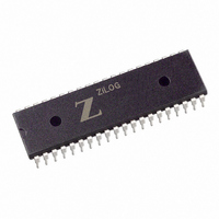
Z0847006PSG Zilog, Z0847006PSG Datasheet - Page 212

Z0847006PSG
Manufacturer Part Number
Z0847006PSG
Description
IC 6MHZ Z80 NMOS DART 40-DIP
Manufacturer
Zilog
Series
Z80r
Datasheet
1.Z0847006PSG.pdf
(330 pages)
Specifications of Z0847006PSG
Processor Type
Z80
Features
Dual Channel Asynchronous Receiver/Transmitter (DART)
Speed
6MHz
Voltage
5V
Mounting Type
Through Hole
Package / Case
40-DIP (0.620", 15.75mm)
Mounting Style
Through Hole
Cpu Speed
6MHz
Digital Ic Case Style
DIP
No. Of Pins
40
Supply Voltage Range
5V
Operating Temperature Range
0°C To +70°C
Svhc
No SVHC (18-Jun-2010)
Base Number
847006
Rohs Compliant
Yes
Clock Frequency
6MHz
Lead Free Status / RoHS Status
Lead free / RoHS Compliant
Available stocks
Company
Part Number
Manufacturer
Quantity
Price
Company:
Part Number:
Z0847006PSG
Manufacturer:
Zilog
Quantity:
22
- Current page: 212 of 330
- Download datasheet (3Mb)
TIMING
UM008101-0601
< % 2 7 2 G T K R J G T C N U
7 U G T / C P W C N
Output Mode (Mode 0)
Only port lines whose mask bit is zero are monitored for generating an
interrupt. When IORQ is high, the forced state of Ready prevents input
register data from changing while the CPU is reading the PIO. Ready goes
High again after the trailing edge of the IORQ, as previously described
Figure 7 illustrates the timing associated with Mode 0 operation. An output
cycle is always started by the execution of an output instruction by the
CPU. A WR
tion and is used to latch the data from the CPU data bus to the addressed
ports (A or B) output register. The rising edge of the WR
the Ready flag after the next falling edge of Φ, indicating that data is avail-
able for the peripheral device. In most systems, the rising edge of the Ready
signal can be used as a latching signal in the peripheral device. The Ready
signal remains active until: (1) a positive edge is received from the strobe
line, indicating that the peripheral has taken the data, or (2) if already
active, Ready is forced low for one and one-half Φ cycles after the leading
edge of IORQ, but only if the port’s output register is written to. Ready
returns High on the first falling edge of Φ after the trailing edge of IORQ.
This guarantees that Ready is low when port data is changing. The Ready
signal does not go inactive until a falling edge occurs on the clock (Φ) line.
The purpose of delaying the negative transition of the Ready signal until
after a negative clock transition is to allow a simple generation scheme for
the strobe pulse. By connecting the Ready line to the Strobe line, a strobe
with a duration of one clock period is generated with no other logic
required. The positive edge of the strobe pulse automatically generates an
INT request when the interrupt enable flip-flop has been set and this device
is the highest priority device requesting an interrupt.
*
pulse is generated by the PIO during a CPU I/O write opera-
Parallel Input/Output
*
pulse then raises
Related parts for Z0847006PSG
Image
Part Number
Description
Manufacturer
Datasheet
Request
R

Part Number:
Description:
Customer Procurement Spec(CPS)
Manufacturer:
ZILOG [Zilog, Inc.]
Datasheet:

Part Number:
Description:
Communication Controllers, ZILOG INTELLIGENT PERIPHERAL CONTROLLER (ZIP)
Manufacturer:
Zilog, Inc.
Datasheet:

Part Number:
Description:
KIT DEV FOR Z8 ENCORE 16K TO 64K
Manufacturer:
Zilog
Datasheet:

Part Number:
Description:
KIT DEV Z8 ENCORE XP 28-PIN
Manufacturer:
Zilog
Datasheet:

Part Number:
Description:
DEV KIT FOR Z8 ENCORE 8K/4K
Manufacturer:
Zilog
Datasheet:

Part Number:
Description:
KIT DEV Z8 ENCORE XP 28-PIN
Manufacturer:
Zilog
Datasheet:

Part Number:
Description:
DEV KIT FOR Z8 ENCORE 4K TO 8K
Manufacturer:
Zilog
Datasheet:

Part Number:
Description:
CMOS Z8 microcontroller. ROM 16 Kbytes, RAM 256 bytes, speed 16 MHz, 32 lines I/O, 3.0V to 5.5V
Manufacturer:
Zilog, Inc.
Datasheet:

Part Number:
Description:
Low-cost microcontroller. 512 bytes ROM, 61 bytes RAM, 8 MHz
Manufacturer:
Zilog, Inc.
Datasheet:

Part Number:
Description:
Z8 4K OTP Microcontroller
Manufacturer:
Zilog, Inc.
Datasheet:

Part Number:
Description:
CMOS SUPER8 ROMLESS MCU
Manufacturer:
Zilog, Inc.
Datasheet:

Part Number:
Description:
SL1866 CMOSZ8 OTP Microcontroller
Manufacturer:
Zilog, Inc.
Datasheet:

Part Number:
Description:
SL1866 CMOSZ8 OTP Microcontroller
Manufacturer:
Zilog, Inc.
Datasheet:

Part Number:
Description:
OTP (KB) = 1, RAM = 125, Speed = 12, I/O = 14, 8-bit Timers = 2, Comm Interfaces Other Features = Por, LV Protect, Voltage = 4.5-5.5V
Manufacturer:
Zilog, Inc.
Datasheet:


