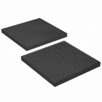
EP1S20F672I7 Altera, EP1S20F672I7 Datasheet - Page 3

EP1S20F672I7
Manufacturer Part Number
EP1S20F672I7
Description
IC STRATIX FPGA 20K LE 672-FBGA
Manufacturer
Altera
Series
Stratix®r
Datasheet
1.EP1S10F780C7.pdf
(276 pages)
Specifications of EP1S20F672I7
Number Of Logic Elements/cells
18460
Number Of Labs/clbs
1846
Total Ram Bits
1669248
Number Of I /o
426
Voltage - Supply
1.425 V ~ 1.575 V
Mounting Type
Surface Mount
Operating Temperature
-40°C ~ 100°C
Package / Case
672-FBGA
Family Name
Stratix
Number Of Logic Blocks/elements
18460
# I/os (max)
426
Frequency (max)
420.17MHz
Process Technology
0.13um (CMOS)
Operating Supply Voltage (typ)
1.5V
Logic Cells
18460
Ram Bits
1669248
Operating Supply Voltage (min)
1.425V
Operating Supply Voltage (max)
1.575V
Operating Temp Range
-40C to 100C
Operating Temperature Classification
Industrial
Mounting
Surface Mount
Pin Count
672
Package Type
FBGA
Lead Free Status / RoHS Status
Contains lead / RoHS non-compliant
Number Of Gates
-
Lead Free Status / Rohs Status
Not Compliant
Available stocks
Company
Part Number
Manufacturer
Quantity
Price
Part Number:
EP1S20F672I7
Manufacturer:
ALTERA/阿尔特拉
Quantity:
20 000
Company:
Part Number:
EP1S20F672I7N
Manufacturer:
ALTERA20
Quantity:
212
Altera Corporation
Chapter
2
3
4
September 2004, v1.1
January 2005, v1.2
January 2006, v3.4
April 2003, v1.0
July 2003, v2.0
July 2005, v1.3
July 2005, v3.3
Date/Version
●
●
●
●
●
●
●
●
●
●
●
●
●
●
●
●
●
●
●
●
●
●
●
●
●
●
Added reference on page 2-73 to Figures 2-50 and 2-51 for
connections.
Updated ranges for EPLL post-scale and pre-scale dividers on page
2-85.
Updated PLL Reconfiguration frequency from 25 to 22 MHz on page
2-87.
New requirement to assert are set signal each PLL when it has to re-
acquire lock on either a new clock after loss of lock (page 2-96).
Updated max input frequency for
Table 2-24.
Renamed impedance matching to series termination throughout.
Updated naming convention for DQS pins on page 2-112 to match pin
tables.
Added DDR SDRAM Performance Specification on page 2-117.
Added external reference resistor values for terminator technology
(page 2-136).
Added Terminator Technology Specification on pages 2-137 and 2-
138.
Updated Tables 2-45 to 2-49 to reflect PLL cross-bank support for
high speed differential channels at full speed.
Wire bond package performance specification for “high” speed
channels was increased to 624 Mbps from 462 Mbps throughout
chapter.
Updated
Updated
Updated
Updated
Updated limits for JTAG chain of devices.
Added new section,
Detection” on page
Updated description of
No new changes in Stratix Device Handbook v2.0.
Added
Updated
Updated
Updated
Updated
Added
Table
Table
“IEEE Std. 1149.1 (JTAG) Boundary-Scan Support”
“Operating Modes”
“Temperature Sensing Diode”
“Configuration”
Tables 4–6
Tables 4–103
Tables 4–114
Table
4–135.
4–130.
4–129.
3–12.
“Stratix Automated Single Event Upset (SEU)
and 4–30.
“Custom-Built Circuitry” on page
through 4–108.
through 4–124.
section.
Changes Made
section.
CLK[1,3,8,10]
Stratix Device Family Data Sheet
section.
from 462 to 500,
3–13.
Section I–3
RCLK
section.


