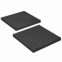
EP1S20F672I7 Altera, EP1S20F672I7 Datasheet - Page 108

EP1S20F672I7
Manufacturer Part Number
EP1S20F672I7
Description
IC STRATIX FPGA 20K LE 672-FBGA
Manufacturer
Altera
Series
Stratix®r
Datasheet
1.EP1S10F780C7.pdf
(276 pages)
Specifications of EP1S20F672I7
Number Of Logic Elements/cells
18460
Number Of Labs/clbs
1846
Total Ram Bits
1669248
Number Of I /o
426
Voltage - Supply
1.425 V ~ 1.575 V
Mounting Type
Surface Mount
Operating Temperature
-40°C ~ 100°C
Package / Case
672-FBGA
Family Name
Stratix
Number Of Logic Blocks/elements
18460
# I/os (max)
426
Frequency (max)
420.17MHz
Process Technology
0.13um (CMOS)
Operating Supply Voltage (typ)
1.5V
Logic Cells
18460
Ram Bits
1669248
Operating Supply Voltage (min)
1.425V
Operating Supply Voltage (max)
1.575V
Operating Temp Range
-40C to 100C
Operating Temperature Classification
Industrial
Mounting
Surface Mount
Pin Count
672
Package Type
FBGA
Lead Free Status / RoHS Status
Contains lead / RoHS non-compliant
Number Of Gates
-
Lead Free Status / Rohs Status
Not Compliant
Available stocks
Company
Part Number
Manufacturer
Quantity
Price
Part Number:
EP1S20F672I7
Manufacturer:
ALTERA/阿尔特拉
Quantity:
20 000
Company:
Part Number:
EP1S20F672I7N
Manufacturer:
ALTERA20
Quantity:
212
- Current page: 108 of 276
- Download datasheet (4Mb)
PLLs & Clock Networks
2–94
Stratix Device Handbook, Volume 1
Any of the four external output counters can drive the single-ended or
differential clock outputs for PLLs 5 and 6. This means one counter or
frequency can drive all output pins available from PLL 5 or PLL 6. Each
pair of output pins (four pins total) has dedicated VCC and GND pins to
reduce the output clock’s overall jitter by providing improved isolation
from switching I/O pins.
For PLLs 5 and 6, each pin of a single-ended output pair can either be in
phase or 180° out of phase. The clock output pin pairs support the same
I/O standards as standard output pins (in the top and bottom banks) as
well as LVDS, LVPECL, 3.3-V PCML, HyperTransport technology,
differential HSTL, and differential SSTL.
standards the enhanced PLL clock pins support. When in single-ended or
differential mode, the two outputs operate off the same power supply.
Both outputs use the same standards in single-ended mode to maintain
performance. You can also use the external clock output pins as user
output pins if external enhanced PLL clocking is not needed.
LVTTL
LVCMOS
2.5 V
1.8 V
1.5 V
3.3-V PCI
3.3-V PCI-X 1.0
LVPECL
3.3-V PCML
LVDS
HyperTransport technology
Differential HSTL
Differential SSTL
3.3-V GTL
3.3-V GTL+
1.5-V HSTL Class I
Table 2–20. I/O Standards Supported for Enhanced PLL Pins (Part 1 of 2)
I/O Standard
INCLK
v
v
v
v
v
v
v
v
v
v
v
v
v
v
v
FBIN
v
v
v
v
v
v
v
v
v
v
v
v
v
v
Table 2–20
Input
PLLENABLE
shows which I/O
v
v
Altera Corporation
EXTCLK
July 2005
Output
v
v
v
v
v
v
v
v
v
v
v
v
v
v
v
v
Related parts for EP1S20F672I7
Image
Part Number
Description
Manufacturer
Datasheet
Request
R

Part Number:
Description:
CYCLONE II STARTER KIT EP2C20N
Manufacturer:
Altera
Datasheet:

Part Number:
Description:
CPLD, EP610 Family, ECMOS Process, 300 Gates, 16 Macro Cells, 16 Reg., 16 User I/Os, 5V Supply, 35 Speed Grade, 24DIP
Manufacturer:
Altera Corporation
Datasheet:

Part Number:
Description:
CPLD, EP610 Family, ECMOS Process, 300 Gates, 16 Macro Cells, 16 Reg., 16 User I/Os, 5V Supply, 15 Speed Grade, 24DIP
Manufacturer:
Altera Corporation
Datasheet:

Part Number:
Description:
Manufacturer:
Altera Corporation
Datasheet:

Part Number:
Description:
CPLD, EP610 Family, ECMOS Process, 300 Gates, 16 Macro Cells, 16 Reg., 16 User I/Os, 5V Supply, 30 Speed Grade, 24DIP
Manufacturer:
Altera Corporation
Datasheet:

Part Number:
Description:
High-performance, low-power erasable programmable logic devices with 8 macrocells, 10ns
Manufacturer:
Altera Corporation
Datasheet:

Part Number:
Description:
High-performance, low-power erasable programmable logic devices with 8 macrocells, 7ns
Manufacturer:
Altera Corporation
Datasheet:

Part Number:
Description:
Classic EPLD
Manufacturer:
Altera Corporation
Datasheet:

Part Number:
Description:
High-performance, low-power erasable programmable logic devices with 8 macrocells, 10ns
Manufacturer:
Altera Corporation
Datasheet:

Part Number:
Description:
Manufacturer:
Altera Corporation
Datasheet:

Part Number:
Description:
Manufacturer:
Altera Corporation
Datasheet:

Part Number:
Description:
Manufacturer:
Altera Corporation
Datasheet:

Part Number:
Description:
CPLD, EP610 Family, ECMOS Process, 300 Gates, 16 Macro Cells, 16 Reg., 16 User I/Os, 5V Supply, 25 Speed Grade, 24DIP
Manufacturer:
Altera Corporation
Datasheet:


