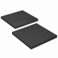
EP1S20F672I7 Altera, EP1S20F672I7 Datasheet - Page 2

EP1S20F672I7
Manufacturer Part Number
EP1S20F672I7
Description
IC STRATIX FPGA 20K LE 672-FBGA
Manufacturer
Altera
Series
Stratix®r
Datasheet
1.EP1S10F780C7.pdf
(276 pages)
Specifications of EP1S20F672I7
Number Of Logic Elements/cells
18460
Number Of Labs/clbs
1846
Total Ram Bits
1669248
Number Of I /o
426
Voltage - Supply
1.425 V ~ 1.575 V
Mounting Type
Surface Mount
Operating Temperature
-40°C ~ 100°C
Package / Case
672-FBGA
Family Name
Stratix
Number Of Logic Blocks/elements
18460
# I/os (max)
426
Frequency (max)
420.17MHz
Process Technology
0.13um (CMOS)
Operating Supply Voltage (typ)
1.5V
Logic Cells
18460
Ram Bits
1669248
Operating Supply Voltage (min)
1.425V
Operating Supply Voltage (max)
1.575V
Operating Temp Range
-40C to 100C
Operating Temperature Classification
Industrial
Mounting
Surface Mount
Pin Count
672
Package Type
FBGA
Lead Free Status / RoHS Status
Contains lead / RoHS non-compliant
Number Of Gates
-
Lead Free Status / Rohs Status
Not Compliant
Available stocks
Company
Part Number
Manufacturer
Quantity
Price
Part Number:
EP1S20F672I7
Manufacturer:
ALTERA/阿尔特拉
Quantity:
20 000
Company:
Part Number:
EP1S20F672I7N
Manufacturer:
ALTERA20
Quantity:
212
Stratix Device Family Data Sheet
Section I–2
Chapter
2
September 2004, v3.1
November 2003, v2.2
October 2003, v2.1
April 2004, v3.0
July 2005 v3.2
Date/Version
●
●
●
●
●
●
●
●
●
●
●
●
●
●
●
●
●
●
●
●
●
●
●
●
●
●
●
●
●
●
●
●
●
●
●
●
●
●
Added
Updated
Format changes.
Updated fast regional clock networks description on
Deleted the word preliminary from the “specification for the maximum
time to relock is 100 µs” on
Added information about differential SSTL and HSTL outputs in
“External Clock Outputs” on page
Updated notes in
Added information about m counter to
Division” on page
Updated Note 1 in
Updated description of
page
Updated
Added references to AN 349 and AN 329 to
Interfacing” on page
Table 2–25 on page
4. Notes 4, 5, and 6, are now Notes 5, 6, and 7, respectively.
Updated
Added information about PCI Compliance to
Table 2–32 on page
Updated reference to device pin-outs now being available on the web
on
Added Notes 4 and 5 to
Updated Note 3 in
Updated Note 5 in
Added note 3 to rows 11 and 12 in
Deleted “Stratix and Stratix GX Device PLL Availability” table.
Added I/O standards row in
strength.
Row
Added checkmarks in Enhanced column for LVPECL, 3.3-V PCML,
LVDS, and HyperTransport technology rows in
Removed the Left and Right I/O Banks row in
Changed
External RAM Interfacing section replaced.
Added 672-pin BGA package information in
Removed support for series and parallel on-chip termination.
Termination Technology renamed differential on-chip termination.
Updated the number of channels per PLL in Tables 2-38 through 2-
42.
Updated
Updated DDR I information.
Updated
Added
Updated
Updated the Lock Detect section.
page
clk [1,3,8,10]
2–88.
“Clear Signals”
Tables
2–130.
“Power Sequencing & Hot Socketing”
Table 2–22 on page
Table 2–26 on page
Figures 2–65
Table
Figures
RCLK
2–25, 2–29, 2–30, and 2–72.
2–22.
values in
2–59, 2–65, and 2–67.
Figure 2–55 on page
2–101.
Table 2–58 on page
Table 2–37 on page
Table 2–41 on page
2–116: updated the table, updated Notes 3 and
2–126: updated the table and deleted Note 1.
2–115.
section.
and 2–67.
“Clock Multiplication & Division” on
Table 2–36 on page
Changes Made
was removed from
Figures 2–50
page
Table 2–28
2–102.
2–117.
Stratix Device Handbook, Volume 1
2–90.
2–92.
Table
“Clock Multiplication &
2–93.
2–101.
2–131.
2–135.
and 2–51.
that support max and min
2–18.
Table
“External RAM
Table
page
2–130.
Table
Table
section.
Altera Corporation
2–37.
2–30.
2–120.
2–34.
page
2–32.
2–73.


