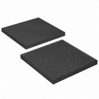
EP1S20F672I7 Altera, EP1S20F672I7 Datasheet - Page 151

EP1S20F672I7
Manufacturer Part Number
EP1S20F672I7
Description
IC STRATIX FPGA 20K LE 672-FBGA
Manufacturer
Altera
Series
Stratix®r
Datasheet
1.EP1S10F780C7.pdf
(276 pages)
Specifications of EP1S20F672I7
Number Of Logic Elements/cells
18460
Number Of Labs/clbs
1846
Total Ram Bits
1669248
Number Of I /o
426
Voltage - Supply
1.425 V ~ 1.575 V
Mounting Type
Surface Mount
Operating Temperature
-40°C ~ 100°C
Package / Case
672-FBGA
Family Name
Stratix
Number Of Logic Blocks/elements
18460
# I/os (max)
426
Frequency (max)
420.17MHz
Process Technology
0.13um (CMOS)
Operating Supply Voltage (typ)
1.5V
Logic Cells
18460
Ram Bits
1669248
Operating Supply Voltage (min)
1.425V
Operating Supply Voltage (max)
1.575V
Operating Temp Range
-40C to 100C
Operating Temperature Classification
Industrial
Mounting
Surface Mount
Pin Count
672
Package Type
FBGA
Lead Free Status / RoHS Status
Contains lead / RoHS non-compliant
Number Of Gates
-
Lead Free Status / Rohs Status
Not Compliant
Available stocks
Company
Part Number
Manufacturer
Quantity
Price
Part Number:
EP1S20F672I7
Manufacturer:
ALTERA/阿尔特拉
Quantity:
20 000
Company:
Part Number:
EP1S20F672I7N
Manufacturer:
ALTERA20
Quantity:
212
- Current page: 151 of 276
- Download datasheet (4Mb)
Figure 2–73. High-Speed Differential I/O Receiver / Transmitter Interface Example
Altera Corporation
July 2005
105 MHz
840 Mbps
R4, R8, and R24
Interconnect
Dedicated
Interface
Receiver
+
–
Fast
PLL
8×
■
■
Dedicated Circuitry
Stratix devices support source-synchronous interfacing with LVDS,
LVPECL, 3.3-V PCML, or HyperTransport signaling at up to 840 Mbps.
Stratix devices can transmit or receive serial channels along with a
low-speed or high-speed clock. The receiving device PLL multiplies the
clock by a integer factor W (W = 1 through 32). For example, a
HyperTransport application where the data rate is 800 Mbps and the
clock rate is 400 MHz would require that W be set to 2. The SERDES factor
J determines the parallel data width to deserialize from receivers or to
serialize for transmitters. The SERDES factor J can be set to 4, 7, 8, or 10
and does not have to equal the PLL clock-multiplication W value. For a J
factor of 1, the Stratix device bypasses the SERDES block. For a J factor of
2, the Stratix device bypasses the SERDES block, and the DDR input and
output registers are used in the IOE. See
An external pin or global or regional clock can drive the fast PLLs, which
can output up to three clocks: two multiplied high-speed differential I/O
clocks to drive the SERDES block and/or external pin, and a low-speed
clock to drive the logic array.
RapidIO
HyperTransport
rx_load_en
Data
8
Interconnect
tx_load_en
Local
8
Data
8
8×
Stratix Device Handbook, Volume 1
Figure
2–73.
Stratix Architecture
Dedicated
Transmitter
Interface
+
–
Regional or
global clock
840 Mbps
2–137
Related parts for EP1S20F672I7
Image
Part Number
Description
Manufacturer
Datasheet
Request
R

Part Number:
Description:
CYCLONE II STARTER KIT EP2C20N
Manufacturer:
Altera
Datasheet:

Part Number:
Description:
CPLD, EP610 Family, ECMOS Process, 300 Gates, 16 Macro Cells, 16 Reg., 16 User I/Os, 5V Supply, 35 Speed Grade, 24DIP
Manufacturer:
Altera Corporation
Datasheet:

Part Number:
Description:
CPLD, EP610 Family, ECMOS Process, 300 Gates, 16 Macro Cells, 16 Reg., 16 User I/Os, 5V Supply, 15 Speed Grade, 24DIP
Manufacturer:
Altera Corporation
Datasheet:

Part Number:
Description:
Manufacturer:
Altera Corporation
Datasheet:

Part Number:
Description:
CPLD, EP610 Family, ECMOS Process, 300 Gates, 16 Macro Cells, 16 Reg., 16 User I/Os, 5V Supply, 30 Speed Grade, 24DIP
Manufacturer:
Altera Corporation
Datasheet:

Part Number:
Description:
High-performance, low-power erasable programmable logic devices with 8 macrocells, 10ns
Manufacturer:
Altera Corporation
Datasheet:

Part Number:
Description:
High-performance, low-power erasable programmable logic devices with 8 macrocells, 7ns
Manufacturer:
Altera Corporation
Datasheet:

Part Number:
Description:
Classic EPLD
Manufacturer:
Altera Corporation
Datasheet:

Part Number:
Description:
High-performance, low-power erasable programmable logic devices with 8 macrocells, 10ns
Manufacturer:
Altera Corporation
Datasheet:

Part Number:
Description:
Manufacturer:
Altera Corporation
Datasheet:

Part Number:
Description:
Manufacturer:
Altera Corporation
Datasheet:

Part Number:
Description:
Manufacturer:
Altera Corporation
Datasheet:

Part Number:
Description:
CPLD, EP610 Family, ECMOS Process, 300 Gates, 16 Macro Cells, 16 Reg., 16 User I/Os, 5V Supply, 25 Speed Grade, 24DIP
Manufacturer:
Altera Corporation
Datasheet:


