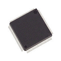
ISP1564HLUM STEricsson, ISP1564HLUM Datasheet - Page 9

ISP1564HLUM
Manufacturer Part Number
ISP1564HLUM
Description
Manufacturer
STEricsson
Datasheet
1.ISP1564HLUM.pdf
(100 pages)
Specifications of ISP1564HLUM
Operating Supply Voltage (typ)
3.3V
Operating Supply Voltage (min)
3V
Operating Supply Voltage (max)
3.6V
Operating Temp Range
-40C to 85C
Operating Temperature Classification
Industrial
Mounting
Surface Mount
Pin Count
100
Lead Free Status / Rohs Status
Compliant
Available stocks
Company
Part Number
Manufacturer
Quantity
Price
NXP Semiconductors
Table 2.
ISP1564_1
Product data sheet
Symbol
AD[11]
V
AD[10]
AD[9]
REG(1V8)
AD[8]
C/BE[0]#
GNDA
AD[7]
AD[6]
GND
AD[5]
AD[4]
AD[3]
AD[2]
AD[1]
AD[0]
V
GNDA
AUX(1V8)
XTAL1
XTAL2
GND
V
OC1_N
CC(IO)
CC(IO)
CC(IO)AUX
[1]
Pin description
Pin
LQFP100 TFBGA100
54
55
56
57
58
59
60
61
62
63
64
65
66
67
68
69
70
71
72
73
74
75
76
77
78
H8
J9
G7
G8
G9
F10
F6
G10
F9
F8
F7
E7
E8
E10
D10
D9
D8
E9
C10
B9
B10
A10
C8
A9
C9
…continued
Type
I/O
-
I/O
I/O
-
I/O
I/O
-
I/O
I/O
-
I/O
I/O
I/O
I/O
I/O
I/O
-
-
-
AI
AO
-
-
I
[2]
Rev. 01 — 4 December 2006
Description
bit 11 of multiplexed PCI address and data
PCI pad; 3.3 V signaling
I/O pads supply voltage; see
bit 10 of multiplexed PCI address and data
PCI pad; 3.3 V signaling
bit 9 of multiplexed PCI address and data
PCI pad; 3.3 V signaling
1.8 V regulator output voltage; only for voltage conditioning; cannot be
used to supply power to external components; see
bit 8 of multiplexed PCI address and data
PCI pad; 3.3 V signaling
byte 0 of multiplexed PCI bus command and byte enable
PCI pad; 3.3 V signaling
analog ground
bit 7 of multiplexed PCI address and data
PCI pad; 3.3 V signaling
bit 6 of multiplexed PCI address and data
PCI pad; 3.3 V signaling
ground
bit 5 of multiplexed PCI address and data
PCI pad; 3.3 V signaling
bit 4 of multiplexed PCI address and data
PCI pad; 3.3 V signaling
bit 3 of multiplexed PCI address and data
PCI pad; 3.3 V signaling
bit 2 of multiplexed PCI address and data
PCI pad; 3.3 V signaling
bit 1 of multiplexed PCI address and data
PCI pad; 3.3 V signaling
bit 0 of multiplexed PCI address and data
PCI pad; 3.3 V signaling
I/O pads supply voltage; see
analog ground
1.8 V auxiliary output voltage; only for voltage conditioning; cannot be
used to supply power to external components; see
crystal oscillator input; this can also be a 12 MHz clock input at 1.8 V
crystal oscillator output (12 MHz); leave open when clock is used
ground
I/O pads auxiliary supply voltage; see
overcurrent sense input for the USB downstream port 1 (digital); when
not in use, connect this pin to 3.3 V
3.3 V input pad; CMOS
Section 7.8
Section 7.8
Section 7.8
HS USB PCI Host Controller
Section 7.8
Section 7.8
© NXP B.V. 2006. All rights reserved.
ISP1564
8 of 99


