ADC12H034CIMSA/NOPB National Semiconductor, ADC12H034CIMSA/NOPB Datasheet - Page 7
ADC12H034CIMSA/NOPB
Manufacturer Part Number
ADC12H034CIMSA/NOPB
Description
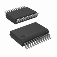
ADC 12BIT W/S&H +SIGN 24-SSOP
Manufacturer
National Semiconductor
Datasheet
1.ADC12030CIWMNOPB.pdf
(42 pages)
Specifications of ADC12H034CIMSA/NOPB
Number Of Bits
12
Data Interface
NSC MICROWIRE™, Serial
Number Of Converters
4
Power Dissipation (max)
33mW
Voltage Supply Source
Analog and Digital
Operating Temperature
-40°C ~ 85°C
Mounting Type
Surface Mount
Package / Case
24-SSOP (0.200", 5.30mm Width)
Number Of Elements
1
Architecture
SAR
Input Polarity
Unipolar
Input Type
Voltage
Rated Input Volt
5V
Differential Input
Yes
Power Supply Requirement
Analog and Digital
Single Supply Voltage (typ)
5V
Single Supply Voltage (min)
4.5V
Single Supply Voltage (max)
5.5V
Dual Supply Voltage (typ)
Not RequiredV
Dual Supply Voltage (min)
Not RequiredV
Dual Supply Voltage (max)
Not RequiredV
Power Dissipation
500mW
Differential Linearity Error
±1LSB
Integral Nonlinearity Error
±1LSB
Operating Temp Range
-40C to 85C
Operating Temperature Classification
Industrial
Mounting
Surface Mount
Pin Count
24
Package Type
SSOP
Lead Free Status / RoHS Status
Lead free / RoHS Compliant
Other names
ADC12H034CIMSA


CCLK, CS, CONV, DI, PD AND SCLK INPUT CHARACTERISTICS
V
V
I
I
DO, EOC AND DOR DIGITAL OUTPUT CHARACTERISTICS
V
V
I
+I
−I
POWER SUPPLY CHARACTERISTICS
I
I
I
Symbol
IN(1)
IN(0)
OUT
D
A
REF
IN(1)
IN(0)
OUT(1)
OUT(0)
+
+
SC
SC
DC and Logic Electrical Characteristics
The following specifications apply for V
mode, f
ADC12032, ADC12034 and ADC12038, R
2.048V common-mode voltage, and 10(t
T
MIN
to T
CK
Logical “1” Input Voltage
Logical “0” Input Voltage
Logical “1” Input Current
Logical “0” Input Current
Logical “1” Output Voltage
Logical “0” Output Voltage
TRI-STATE Output Current
Output Short Circuit Source Current
Output Short Circuit Sink Current
Digital Supply Current
ADC12030, ADC12032, ADC12034 and
ADC12038
Digital Supply Current
ADC12H030, ADC12H032, ADC12H034
and ADC12H038
Positive Analog Supply Current
Reference Input Current
MAX
= f
; all other limits T
SK
= 8 MHz for the ADC12H030, ADC12H032, ADC12H034 and ADC12H038, f
Parameter
A
= T
J
= 25°C. (Notes 7, 8, 9)
+
CK
= V
S
) acquisition time unless otherwise specified. Boldface limits apply for T
= 25Ω, source impedance for V
A
+ = V
V
V
V
V
V
V
V
V
V
V
V
Awake
CS = HIGH, Powered Down, CCLK on
CS = HIGH, Powered Down, CCLK off
Awake
CS = HIGH, Powered Down, CCLK on
CS = HIGH, Powered Down, CCLK off
Awake
CS = HIGH, Powered Down, CCLK on
CS = HIGH, Powered Down, CCLK off
Awake
CS = HIGH, Powered Down
D
+
+
IN
IN
+
+
+
OUT
OUT
OUT
OUT
+ = +5.0 V
= 5.5V
= 4.5V
= 4.5V, I
= 4.5V, I
= 4.5V, I
= 5.0V
= 0V
= 0V
= 5V
= 0V
= V
D
+
OUT
OUT
OUT
DC
7
Conditions
, V
= −360 µA
= − 10 µA
= 1.6 mA
REF
+ = +4.096 V
REF
+ and V
DC
REF
, V
−
REF
≤
− = 0 V
CK
(Note 10)
25Ω, fully-differential input with fixed
Typical
−0.005
0.005
−0.1
= f
600
0.1
1.6
2.3
0.9
2.7
0.1
0.1
14
16
20
20
10
70
SK
DC
= 5 MHz for the ADC12030,
, 12-bit + sign conversion
(Note 11)
Limits
−1.0
4.25
−3.0
2.0
0.8
1.0
2.4
0.4
3.0
6.5
8.0
2.5
3.2
4.0
A
www.national.com
= T
mA (max)
mA (max)
µA (max)
µA (max)
µA (max)
mA (min)
mA (min)
µA (min)
(Limits)
V (max)
V (max)
V (min)
V (min)
V (min)
Units
J
mA
mA
µA
µA
µA
µA
µA
µA
µA
=
Related parts for ADC12H034CIMSA/NOPB
Image
Part Number
Description
Manufacturer
Datasheet
Request
R

Part Number:
Description:
National Semiconductor [8-Bit D/A Converter]
Manufacturer:
National Semiconductor
Datasheet:
Part Number:
Description:
National Semiconductor [Media Coprocessor]
Manufacturer:
National Semiconductor
Datasheet:
Part Number:
Description:
Digitally Controlled Tone and Volume Circuit with Stereo Audio Power Amplifier, Microphone Preamp Stage and National 3D Sound
Manufacturer:
National Semiconductor
Datasheet:
Part Number:
Description:
Digitally Controlled Tone and Volume Circuit with Stereo Audio Power Amplifier, Microphone Preamp Stage and National 3D Sound
Manufacturer:
National Semiconductor
Datasheet:
Part Number:
Description:
AC97 Rev 2 Codec with Sample Rate Conversion and National 3D Sound
Manufacturer:
National Semiconductor
Part Number:
Description:
Manufacturer:
National Semiconductor
Datasheet:
Part Number:
Description:
Manufacturer:
National Semiconductor
Datasheet:
Part Number:
Description:
General Purpose, Low Voltage, Low Power, Rail-to-Rail Output Operational Amplifiers
Manufacturer:
National Semiconductor
Datasheet:
Part Number:
Description:
8-bit 20 MSPS flash A/D converter.
Manufacturer:
National Semiconductor
Datasheet:
Part Number:
Description:
Low Noise Quad Operational Amplifier
Manufacturer:
National Semiconductor
Datasheet:
Part Number:
Description:
Quad Differential Line Receivers
Manufacturer:
National Semiconductor
Datasheet:
Part Number:
Description:
Quad High Speed Trapezoidal? Bus Transceiver
Manufacturer:
National Semiconductor
Datasheet:
Part Number:
Description:
Dual Line Receiver
Manufacturer:
National Semiconductor
Datasheet:
Part Number:
Description:
TTL to 10k ECL Level Translator with Latch
Manufacturer:
National Semiconductor
Datasheet: