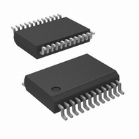
ADC12H034CIMSA/NOPB National Semiconductor, ADC12H034CIMSA/NOPB Datasheet - Page 5

ADC12H034CIMSA/NOPB
Manufacturer Part Number
ADC12H034CIMSA/NOPB
Description
ADC 12BIT W/S&H +SIGN 24-SSOP
Manufacturer
National Semiconductor
Datasheet
1.ADC12030CIWMNOPB.pdf
(42 pages)
Specifications of ADC12H034CIMSA/NOPB
Number Of Bits
12
Data Interface
NSC MICROWIRE™, Serial
Number Of Converters
4
Power Dissipation (max)
33mW
Voltage Supply Source
Analog and Digital
Operating Temperature
-40°C ~ 85°C
Mounting Type
Surface Mount
Package / Case
24-SSOP (0.200", 5.30mm Width)
Number Of Elements
1
Architecture
SAR
Input Polarity
Unipolar
Input Type
Voltage
Rated Input Volt
5V
Differential Input
Yes
Power Supply Requirement
Analog and Digital
Single Supply Voltage (typ)
5V
Single Supply Voltage (min)
4.5V
Single Supply Voltage (max)
5.5V
Dual Supply Voltage (typ)
Not RequiredV
Dual Supply Voltage (min)
Not RequiredV
Dual Supply Voltage (max)
Not RequiredV
Power Dissipation
500mW
Differential Linearity Error
±1LSB
Integral Nonlinearity Error
±1LSB
Operating Temp Range
-40C to 85C
Operating Temperature Classification
Industrial
Mounting
Surface Mount
Pin Count
24
Package Type
SSOP
Lead Free Status / RoHS Status
Lead free / RoHS Compliant
Other names
ADC12H034CIMSA
STATIC CONVERTER CHARACTERISTICS
ILE
DNL
TUE
INL
DNL
Symbol
Absolute Maximum Ratings
(Notes 1, 2)
If Military/Aerospace specified devices are required,
please contact the National Semiconductor Sales Office/
Distributors for availability and specifications.
Converter Electrical Characteristics
The following specifications apply for V
mode, f
ADC12032, ADC12034 and ADC12038, R
2.048V common-mode voltage, and 10(t
T
Positive Supply Voltage
Voltage at Inputs and Outputs
Voltage at Analog Inputs
|V
Input Current at Any Pin (Note 3)
Package Input Current (Note 3)
Package Dissipation at
ESD Susceptibility (Note 5)
Soldering Information
Storage Temperature
MIN
A
(V
except CH0–CH7 and COM
CH0–CH7 and COM
T
Human Body Model
N Packages (10 seconds)
SO Package (Note 6):
+ − V
A
to T
+
Vapor Phase (60 seconds)
Infrared (15 seconds)
= 25°C (Note 4)
= V
CK
Resolution with No Missing Codes
Integral Linearity Error
Differential Non-Linearity
Positive Full-Scale Error
Negative Full-Scale Error
Offset Error
DC Common Mode Error
Total Unadjusted Error
Resolution with No Missing Codes 8-bit + sign mode
Integral Linearity Error
Differential Non-Linearity
Positive Full-Scale Error
Negative Full-Scale Error
MAX
D
A
= f
+|
+ = V
; all other limits T
SK
= 8 MHz for the ADC12H030, ADC12H032, ADC12H034 and ADC12H038, f
D
+)
Parameter
A
= T
J
= 25°C. (Notes 7, 8, 9)
GND −5V to (V
+
−0.3V to (V
CK
= V
S
−65°C to +150°C
) acquisition time unless otherwise specified. Boldface limits apply for T
= 25Ω, source impedance for V
A
After Auto Cal (Notes 12, 18)
After Auto Cal
After Auto Cal (Notes 12, 18)
After Auto Cal (Notes 12, 18)
After Auto Cal (Notes 5, 18)
V
After Auto Cal (Note 15)
After Auto Cal (Notes 12, 13, 14)
8-bit + sign mode (Note 12)
8-bit + sign mode
8-bit + sign mode (Note 12)
8-bit + sign mode (Note 12)
+ = V
IN
(+) = V
±120 mA
D
500 mW
+
±30 mA
300 mV
+ = +5.0 V
+0.3V)
1500V
+
260°C
215°C
220°C
+5V)
6.5V
IN
(−) = 2.048V
Conditions
DC
5
, V
Operating Temperature Range
Supply Voltage (V
|V
V
V
V
V
A/DIN1, A/DIN2, MUXOUT1 and
MUXOUT2 Voltage Range
REF
Operating Ratings
Package Thermal Resistance
NOTE: Some of these devices may be obsolete or on
Lifetime Buy status. Check our web site for product avail-
ability.
REF
REF
REF
REF
A
IN Common Mode Voltage Range
ADC12(H)030CIWM
ADC12032CIWM
ADC12034CIN
ADC12034CIWM
ADC12H034CIMSA
ADC12(H)038CIWM
+ − V
+ = +4.096 V
+
−
(V
Common Mode Voltage Range
[(V
[(V
REF
REF
D
+|
REF
IN
+ and V
+ − V
+) − (V
+) − (V
Part Number
REF
DC
+
IN
REF
, V
−)
= V
REF
−)] / 2
−
REF
A
−)] / 2
≤
+ = V
(Note 10)
− = 0 V
CK
Typical
25Ω, fully-differential input with fixed
±1/2
±1/2
±1/2
±1/2
±2
±1
= f
D
SK
+)
DC
= 5 MHz for the ADC12030,
(Notes 1, 2)
, 12-bit + sign conversion
Thermal Resistance
12 + sign
(Note 11)
8 + sign
Limits
±3.0
±3.0
±3.5
±1/2
±3/4
±1/2
±1/2
−40°C
±1
±1
±2
0.1 V
0V to (V
T
70°C/W
64°C/W
42°C/W
57°C/W
97°C/W
50°C/W
MIN
(θ
+4.5V to +5.5V
≤
JA
A
A
www.national.com
≤
+ to 0.6 V
)
T
= T
LSB (max)
LSB (max)
LSB (max)
LSB (max)
LSB (max)
LSB (max)
LSB (max)
LSB (max)
LSB (max)
LSB (max)
T
A
REF
≤
0V to V
1V to V
0V to V
0V to V
Bits (min)
Bits (min)
(Limits)
A
≤
J
Units
100 mV
≤
LSB
+ −1V)
=
+85°C
T
MAX
A
A
A
A
A
+
+
+
+
+


