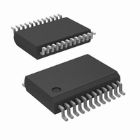
ADC12H034CIMSA/NOPB National Semiconductor, ADC12H034CIMSA/NOPB Datasheet - Page 27

ADC12H034CIMSA/NOPB
Manufacturer Part Number
ADC12H034CIMSA/NOPB
Description
ADC 12BIT W/S&H +SIGN 24-SSOP
Manufacturer
National Semiconductor
Datasheet
1.ADC12030CIWMNOPB.pdf
(42 pages)
Specifications of ADC12H034CIMSA/NOPB
Number Of Bits
12
Data Interface
NSC MICROWIRE™, Serial
Number Of Converters
4
Power Dissipation (max)
33mW
Voltage Supply Source
Analog and Digital
Operating Temperature
-40°C ~ 85°C
Mounting Type
Surface Mount
Package / Case
24-SSOP (0.200", 5.30mm Width)
Number Of Elements
1
Architecture
SAR
Input Polarity
Unipolar
Input Type
Voltage
Rated Input Volt
5V
Differential Input
Yes
Power Supply Requirement
Analog and Digital
Single Supply Voltage (typ)
5V
Single Supply Voltage (min)
4.5V
Single Supply Voltage (max)
5.5V
Dual Supply Voltage (typ)
Not RequiredV
Dual Supply Voltage (min)
Not RequiredV
Dual Supply Voltage (max)
Not RequiredV
Power Dissipation
500mW
Differential Linearity Error
±1LSB
Integral Nonlinearity Error
±1LSB
Operating Temp Range
-40C to 85C
Operating Temperature Classification
Industrial
Mounting
Surface Mount
Pin Count
24
Package Type
SSOP
Lead Free Status / RoHS Status
Lead free / RoHS Compliant
Other names
ADC12H034CIMSA
MUX Address
ADC12038
ADC12034
ADC12030
ADC12032
DI0
Note: ADC12030 and ADC12H030 do not have A/DIN1, A/DIN2, MUX-
Note: The ADC powers up with no Auto Cal, no Auto Zero, 10 CCLK acquisition time, 12-bit + sign conversion, power up, 12- or 13-bit MSB first, and user mode.
X = Don't Care
X = Don't Care
H
H
L
L
and
OUT1 and MUXOUT2 pins.
DI1
H
H
L
L
See Tables 2, 3 or Table 4
See Tables 2, 3 or Table 4
See Tables 2, 3 or Table 4
See Tables 2, 3 or Table 4
See Tables 2, 3 or Table 4
See Tables 2, 3 or Table 4
DI0
DI0
DI0
H
H
H
H
L
L
L
L
L
L
L
L
L
L
L
CH0
+
−
+
with A/DIN1 tied to MUXOUT1
and A/DIN2 tied to MUXOUT2
DI1
DI1
DI1
Analog Channel Addressed
CS
H
H
X
L
L
L
L
L
L
L
L
L
L
L
L
H
X
L
L
and Assignment
CONV
DI2
DI2
X
L
L
L
L
L
L
L
L
L
L
L
L
L
L
H
X
X
L
TABLE 4. ADC12032 and ADC12030 Multiplexer Addressing
TABLE 6. Conversion/Read Data Only Mode Programming
CH1
−
+
+
DI3
X
L
L
L
L
L
L
L
L
L
L
L
L
L
L
PD
H
L
L
L
DI4
DI3
DI2
H
H
H
H
H
H
H
H
H
H
H
H
H
L
L
L
L
L
L
L
L
TABLE 5. Mode Programming
DI5
DI4
DI3
COM
H
H
H
H
H
H
H
H
H
H
H
H
H
L
L
L
L
L
L
L
L
Read Only (Previous DO Format). No Conversion.
−
−
DI6
DI5
DI4
H
H
H
H
H
H
H
H
H
H
H
H
L
L
L
L
L
L
L
L
L
ADC Input Polarity
DI7
DI6
DI5
A/DIN1
H
H
H
H
H
H
H
H
H
H
L
L
L
L
L
L
L
L
L
L
L
27
+
−
+
+
Assignment
See Table 5 for Mode
(CH1–CH7 become Active Outputs)
Acquisition Time—10 CCLK Cycles
Acquisition Time—18 CCLK Cycles
Acquisition Time—34 CCLK Cycles
Acquisition Time—6 CCLK Cycles
Power Down
12 Bit Conversion of Full-Scale
12 Bit Conversion of Offset
Mode
A/DIN2
Idle
Data Out without Sign
Read Status Register
Data Out with Sign
−
+
−
−
12 Bit Conversion
12 Bit Conversion
12 Bit Conversion
12 Bit Conversion
8 Bit Conversion
8 Bit Conversion
Mode Selected
Power Down
User Mode
Test Mode
(Current)
Auto Zero
Power Up
Auto Cal
MUXOUT1
Channel Assignment
Multiplexer Output
CH0
CH0
CH0
CH1
MUXOUT2
COM
COM
CH1
CH1
12 or 13 Bit MSB First
16 or 17 Bit MSB First
12 or 13 Bit MSB First
12 or 13 Bit LSB First
16 or 17 Bit LSB First
12 or 13 Bit LSB First
8 or 9 Bit MSB First
8 or 9 Bit LSB First
(next Conversion
DO Format
No Change
No Change
No Change
No Change
No Change
No Change
No Change
No Change
No Change
No Change
No Change
No Change
No Change
Single-Ended
Cycle)
Differential
www.national.com
Mode


