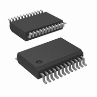
ADC12H034CIMSA/NOPB National Semiconductor, ADC12H034CIMSA/NOPB Datasheet - Page 34

ADC12H034CIMSA/NOPB
Manufacturer Part Number
ADC12H034CIMSA/NOPB
Description
ADC 12BIT W/S&H +SIGN 24-SSOP
Manufacturer
National Semiconductor
Datasheet
1.ADC12030CIWMNOPB.pdf
(42 pages)
Specifications of ADC12H034CIMSA/NOPB
Number Of Bits
12
Data Interface
NSC MICROWIRE™, Serial
Number Of Converters
4
Power Dissipation (max)
33mW
Voltage Supply Source
Analog and Digital
Operating Temperature
-40°C ~ 85°C
Mounting Type
Surface Mount
Package / Case
24-SSOP (0.200", 5.30mm Width)
Number Of Elements
1
Architecture
SAR
Input Polarity
Unipolar
Input Type
Voltage
Rated Input Volt
5V
Differential Input
Yes
Power Supply Requirement
Analog and Digital
Single Supply Voltage (typ)
5V
Single Supply Voltage (min)
4.5V
Single Supply Voltage (max)
5.5V
Dual Supply Voltage (typ)
Not RequiredV
Dual Supply Voltage (min)
Not RequiredV
Dual Supply Voltage (max)
Not RequiredV
Power Dissipation
500mW
Differential Linearity Error
±1LSB
Integral Nonlinearity Error
±1LSB
Operating Temp Range
-40C to 85C
Operating Temperature Classification
Industrial
Mounting
Surface Mount
Pin Count
24
Package Type
SSOP
Lead Free Status / RoHS Status
Lead free / RoHS Compliant
Other names
ADC12H034CIMSA
www.national.com
3.0 REFERENCE VOLTAGE
The difference in the voltages applied to the V
V
the voltage applied between two multiplexer inputs or the
voltage applied to one of the multiplexer inputs and analog
ground) over which 4095 positive and 4096 negative codes
exist. The voltage sources driving V
very low output impedance and noise. The circuit in is an
example of a very stable reference appropriate for use with
the device.
*Tantalum
The ADC12030/2/4/8 can be used in either ratiometric or ab-
solute reference applications. In ratiometric systems, the ana-
log input voltage is proportional to the voltage used for the
ADC's reference voltage. When this voltage is the system
power supply, the V
connected to ground. This technique relaxes the system ref-
erence stability requirements because the analog input volt-
age and the ADC reference voltage move together. This
maintains the same output code for given input conditions.
For absolute accuracy, where the analog input voltage varies
between very specific voltage limits, a time and temperature
stable voltage source can be connected to the reference in-
puts. Typically, the reference voltage magnitude will require
an initial adjustment to null reference voltage induced full-
scale errors.
Below are recommended references along with some key
specifications.
REF
−
defines the analog input span (the difference between
FIGURE 16. Low Drift Extremely
Stable Reference Circuit
REF
+
pin is connected to V
REF
+
and V
FIGURE 15. Fully Differential Biasing
REF
A
+
and V
−
must have
REF
REF
+
1135442
and
−
is
34
The reference voltage inputs are not fully differential. The
ADC12030/2/4/8 will not generate correct conversions or
comparisons if V
sions result when V
remain at all times between ground and V
mon mode range, (V
V
reference ladder should not go below 0.5V or above 3.0V.
Figure 17 is a graphic representation of the voltage restric-
tions on V
LM4041CI-Adj
LM4040AI-4.1
LM4120AI-4.1
LM4121AI-4.1
LM4050AI-4.1
LM4030AI-4.1
LM4140AC-4.1
Circuit of Figure 16
A
+
) to (0.6 × V
Part Number
REF
+
and V
A
+
REF
). Therefore, with V
REF
+
REF
REF
is taken below V
+
−
and V
+
.
+ V
Tolerance
Adjustable
REF
REF
Voltage
±0.05%
Output
±0.5%
±0.1%
±0.2%
±0.2%
±0.1%
±0.1%
−
−
)/2, is restricted to (0.1 ×
differ by 1V or more and
A
+
REF
= 5V the center of the
1135450
A
−
. Correct conver-
+
. The V
Temperature
Coefficient
±100ppm/°C
±100ppm/°C
±3.0ppm/°C
±50ppm/°C
±50ppm/°C
±50ppm/°C
±10ppm/°C
±2ppm/°C
REF
com-


