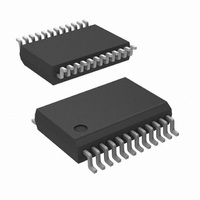
ADC12H034CIMSA/NOPB National Semiconductor, ADC12H034CIMSA/NOPB Datasheet - Page 10

ADC12H034CIMSA/NOPB
Manufacturer Part Number
ADC12H034CIMSA/NOPB
Description
ADC 12BIT W/S&H +SIGN 24-SSOP
Manufacturer
National Semiconductor
Datasheet
1.ADC12030CIWMNOPB.pdf
(42 pages)
Specifications of ADC12H034CIMSA/NOPB
Number Of Bits
12
Data Interface
NSC MICROWIRE™, Serial
Number Of Converters
4
Power Dissipation (max)
33mW
Voltage Supply Source
Analog and Digital
Operating Temperature
-40°C ~ 85°C
Mounting Type
Surface Mount
Package / Case
24-SSOP (0.200", 5.30mm Width)
Number Of Elements
1
Architecture
SAR
Input Polarity
Unipolar
Input Type
Voltage
Rated Input Volt
5V
Differential Input
Yes
Power Supply Requirement
Analog and Digital
Single Supply Voltage (typ)
5V
Single Supply Voltage (min)
4.5V
Single Supply Voltage (max)
5.5V
Dual Supply Voltage (typ)
Not RequiredV
Dual Supply Voltage (min)
Not RequiredV
Dual Supply Voltage (max)
Not RequiredV
Power Dissipation
500mW
Differential Linearity Error
±1LSB
Integral Nonlinearity Error
±1LSB
Operating Temp Range
-40C to 85C
Operating Temperature Classification
Industrial
Mounting
Surface Mount
Pin Count
24
Package Type
SSOP
Lead Free Status / RoHS Status
Lead free / RoHS Compliant
Other names
ADC12H034CIMSA
www.national.com
Note 8: To guarantee accuracy, it is required that the V
V
Note 9: With the test condition for V
Note 10: Typical figures are at T
Note 11: Tested limits are guaranteed to National's AOQL (Average Outgoing Quality Level).
Note 12: Positive integral linearity Error is defined as the deviation of the analog value, expressed in LSBs, from the straight line that passes through positive
full-scale and zero. For Negative Integral Linearity Error, the straight line passes through negative full-scale and zero (see Figures 2, 3).
Note 13: Offset error is a measure of the deviation from the mid-scale voltage (a code of zero), expressed in LSB. It is the worst-case value of the code transitions
between 1 to 0 and 0 to +1 (see Figure 4).
Note 14: Total unadjusted error includes offset, full-scale, linearity and multiplexer errors.
Note 15: The DC common-mode error is measured in the differential multiplexer mode with the assigned positive and negative input channels shorted together.
Note 16: Channel leakage current is measured after the channel selection.
Note 17: Timing specifications are tested at the TTL logic levels, V
to 1.4V.
Note 18: The ADC12030 family's self-calibration technique ensures linearity and offset errors as specified, but noise inherent in the self-calibration process will
result in a maximum repeatability uncertainty of 0.2 LSB.
Note 19: If SCLK and CCLK are driven from the same clock source, then t
Note 20: The “12-Bit Conversion of Offset” and “12-Bit Conversion of Full-Scale” modes are intended to test the functionality of the device. Therefore, the output
data from these modes are not an indication of the accuracy of a conversion result.
+
pin.
J
= T
REF
A
= 25°C and represent most likely parametric norm.
(V
REF
+ − V
REF
−) given as +4.096V, the 12-bit LSB is 1.0 mV and the 8-bit LSB is 16.0 mV.
A
+ and V
FIGURE 1. Transfer Characteristic
D
+ be connected together to the same power supply with separate bypass capacitors at each
IL
= 0.4V for a falling edge and V
A
is 6, 10, 18 or 34 clock periods minimum and maximum.
10
IH
1135402
= 2.4V for a rising edge. TRI-STATE output voltage is forced
1135410


