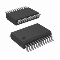
ADC12H034CIMSA/NOPB National Semiconductor, ADC12H034CIMSA/NOPB Datasheet - Page 31

ADC12H034CIMSA/NOPB
Manufacturer Part Number
ADC12H034CIMSA/NOPB
Description
ADC 12BIT W/S&H +SIGN 24-SSOP
Manufacturer
National Semiconductor
Datasheet
1.ADC12030CIWMNOPB.pdf
(42 pages)
Specifications of ADC12H034CIMSA/NOPB
Number Of Bits
12
Data Interface
NSC MICROWIRE™, Serial
Number Of Converters
4
Power Dissipation (max)
33mW
Voltage Supply Source
Analog and Digital
Operating Temperature
-40°C ~ 85°C
Mounting Type
Surface Mount
Package / Case
24-SSOP (0.200", 5.30mm Width)
Number Of Elements
1
Architecture
SAR
Input Polarity
Unipolar
Input Type
Voltage
Rated Input Volt
5V
Differential Input
Yes
Power Supply Requirement
Analog and Digital
Single Supply Voltage (typ)
5V
Single Supply Voltage (min)
4.5V
Single Supply Voltage (max)
5.5V
Dual Supply Voltage (typ)
Not RequiredV
Dual Supply Voltage (min)
Not RequiredV
Dual Supply Voltage (max)
Not RequiredV
Power Dissipation
500mW
Differential Linearity Error
±1LSB
Integral Nonlinearity Error
±1LSB
Operating Temp Range
-40C to 85C
Operating Temperature Classification
Industrial
Mounting
Surface Mount
Pin Count
24
Package Type
SSOP
Lead Free Status / RoHS Status
Lead free / RoHS Compliant
Other names
ADC12H034CIMSA
1.7 Reading the Data Without Starting a Conversion
The data from a particular conversion may be accessed with-
out starting a new conversion by ensuring that the CONV line
is taken high during the I/O sequence. See the Read Data
timing diagrams. Table 6 describes the operation of the
CONV pin. It is not necessary to read the data as soon as
DOR goes low. The data will remain in the output register if
CS is brought high right after DOR goes high. A single con-
version may be read as many times as desired before CS is
brought low.
1.8 Brown Out Conditions
When the supply voltage dips below about 2.7V, the internal
registers, including the calibration coefficients and all of the
other registers, may lose their contents. When this happens
the ADC will not perform as expected or not at all after power
A/DIN1 and A/DIN2 can be assigned as the + or − input
CH0, CH2, CH4, and CH6 can be assigned to the MUXOUT1
pin in the differential configuration, while CH1, CH3, CH5, and
CH7 can be assigned to the MUXOUT2 pin. In the differential
configuration, the analog inputs are paired as follows: CH0
with CH1, CH2 with CH3, CH4 with CH5 and CH6 with CH7.
The A/DIN1 and A/DIN2 pins can be assigned positive or
negative polarity.
With the single-ended multiplexer configuration, CH0 through
CH7 can be assigned to the MUXOUT1 pin. The COM pin is
always assigned to the MUXOUT2 pin. A/DIN1 is assigned as
Configuration
4 Differential
Differential
Channels
FIGURE 10. MUXOUT connections for multiplexer option
1135438
1135440
FIGURE 9. Input Multiplexer Options
31
A/DIN1 is + input
A/DIN2 is − input
is fully restored. While writing the desired information to all
registers and performing a calibration might sometimes cause
recovery to full operation, the only sure recovery method is to
reduce the supply voltage to below 0.5V, then reprogram the
ADC and perform a calibration after power is fully restored.
2.0 THE ANALOG MULTIPLEXER
For the ADC12038, the analog input multiplexer can be con-
figured with 4 differential channels or 8 single ended channels
with the COM input as the zero reference or any combination
thereof (see Figure 9). The difference between the voltages
at the V
(V
digital output codes result when V
age at V
the positive input; A/DIN2 is assigned as the negative input.
(See Figure 10).
The Multiplexer assignment tables for these ADCs (Tables
2, 3, 4) summarize the aforementioned functions for the dif-
ferent versions of ADCs.
2.1 Biasing for Various Multiplexer Configurations
Figure 11 is an example of device connections for single-
ended operation. The sign bit is always low. The digital output
range is 0 0000 0000 0000 to 0 1111 1111 1111. One LSB is
equal to 1 mV (4.1V/4096 LSBs).
REF
). The analog input voltage range is 0 to V
REF
IN
−
+
or V
and V
8 Single-Ended Channels
IN
+
REF
as Zero Reference
cannot go below AGND.
Configuration
Single-Ended
−
pins determines the input voltage span
with COM
1135439
IN
−
1135441
> V
IN
+
. The actual volt-
A
www.national.com
+
. Negative


