ADC12H034CIMSA/NOPB National Semiconductor, ADC12H034CIMSA/NOPB Datasheet - Page 6
ADC12H034CIMSA/NOPB
Manufacturer Part Number
ADC12H034CIMSA/NOPB
Description
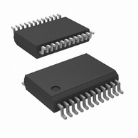
ADC 12BIT W/S&H +SIGN 24-SSOP
Manufacturer
National Semiconductor
Datasheet
1.ADC12030CIWMNOPB.pdf
(42 pages)
Specifications of ADC12H034CIMSA/NOPB
Number Of Bits
12
Data Interface
NSC MICROWIRE™, Serial
Number Of Converters
4
Power Dissipation (max)
33mW
Voltage Supply Source
Analog and Digital
Operating Temperature
-40°C ~ 85°C
Mounting Type
Surface Mount
Package / Case
24-SSOP (0.200", 5.30mm Width)
Number Of Elements
1
Architecture
SAR
Input Polarity
Unipolar
Input Type
Voltage
Rated Input Volt
5V
Differential Input
Yes
Power Supply Requirement
Analog and Digital
Single Supply Voltage (typ)
5V
Single Supply Voltage (min)
4.5V
Single Supply Voltage (max)
5.5V
Dual Supply Voltage (typ)
Not RequiredV
Dual Supply Voltage (min)
Not RequiredV
Dual Supply Voltage (max)
Not RequiredV
Power Dissipation
500mW
Differential Linearity Error
±1LSB
Integral Nonlinearity Error
±1LSB
Operating Temp Range
-40C to 85C
Operating Temperature Classification
Industrial
Mounting
Surface Mount
Pin Count
24
Package Type
SSOP
Lead Free Status / RoHS Status
Lead free / RoHS Compliant
Other names
ADC12H034CIMSA


www.national.com
TUE
UNIPOLAR DYNAMIC CONVERTER CHARACTERISTICS
S/(N+D)
DIFFERENTIAL DYNAMIC CONVERTER CHARACTERISTICS
S/(N+D)
REFERENCE INPUT, ANALOG INPUTS AND MULTIPLEXER CHARACTERISTICS
C
C
C
C
Symbol
REF
A/D
CH
MUXOUT
R
ON
Offset Error
Total Unadjusted Error
Multiplexer Chan-to-Chan
Matching
Power Supply Sensitivity
Output Data from “12-Bit
Conversion of Offset”
Output Data from “12-Bit
Conversion of Full-Scale”
Signal-to-Noise Plus Distortion
Ratio
−3 dB Full Power Bandwidth
Signal-to-Noise Plus Distortion
Ratio
−3 dB Full Power Bandwidth
Reference Input Capacitance
A/DIN1, A/DIN2 Analog Input
Capacitance
A/DIN1, A/DIN2 Analog Input
Leakage Current
CH0–CH7 and COM Input Voltage
CH0–CH7 and COM Input
Capacitance
MUX Output Capacitance
Off Channel Leakage CH0–CH7
and COM Pins (Note 16)
On Channel Leakage CH0–CH7
and COM Pins (Note 16)
MUXOUT1 and MUXOUT2
Leakage Current
MUX On Resistance
R
Chan-to-Chan Crosstalk
MUX Bandwidth
ON
Matching Chan-to-Chan
Parameter
Integral Linearity Error
+ Full-Scale Error
− Full-Scale Error
Offset Error
8-bit + sign mode, after Auto Zero
V
8-bit + sign mode after Auto Zero
(Notes 12, 13, 14)
V
(see Table 5) (Note 20)
(see Table 5) (Note 20)
f
f
f
V
f
f
f
V
V
On Channel = 5V and Off Channel = 0V
On Channel = 0V and Off Channel = 5V
On Channel = 5V and Off Channel = 0V
On Channel = 0V and Off Channel = 5V
V
V
V
V
IN
IN
IN
IN
IN
IN
IN
+
IN
IN
IN
MUXOUT
IN
IN
IN
= 1 kHz, V
= 20 kHz, V
= 40 kHz, V
= 1 kHz, V
= 20 kHz, V
= 40 kHz, V
= +5V ±10%, V
(+) = V
= 5 V
= ±5V, where S/(N+D) drops 3 dB
= +5.0V or V
= 2.5V and V
= 2.5V and V
= 5 V
P-P
= 5.0V or V
P-P
IN
(−) = + 2.048V (Note 13)
, where S/(N+D) drops 3 dB
, f
IN
IN
IN
IN
IN
IN
IN
= 5 V
= ±5V, V
= 40 kHz
Conditions
IN
= 5 V
= 5 V
= ±5V, V
= ±5V, V
MUXOUT
MUXOUT
REF
6
= 0V
MUXOUT
P-P
= +4.096V
P-P
P-P
, V
REF
= 2.4V
= 2.4V
, V
, V
REF
REF
REF
REF
REF
+
= 0V
+
+
= 5.0V
+
= 5.0V
= 5.0V
+
+ = 5.0V
= 5.0V
= 5.0V
(Note 10)
Typical
±0.05
−0.01
−0.01
±0.5
±0.5
±0.5
±0.5
69.4
68.3
65.7
77.0
73.9
67.0
±0.1
0.01
0.01
0.01
850
−72
31
40
85
75
10
20
90
5
(V
GND − 0.05
(Note 11)
A
Limits
+) + 0.05
4095
4093
1150
±1/2
±3/4
±1.5
±1.5
±1.0
−0.3
−0.3
+10
−10
0.3
0.3
0.3
±1
LSB (max)
LSB (max)
LSB (max)
LSB (max)
LSB (max)
LSB (max)
LSB (max)
LSB (min)
LSB (min)
µA (max)
µA (max)
µA (max)
µA (max)
µA (min)
µA (min)
(Limits)
V (max)
Ω (max)
V (min)
Units
LSB
LSB
kHz
kHz
kHz
dB
dB
dB
dB
dB
dB
pF
pF
pF
pF
dB
%
Related parts for ADC12H034CIMSA/NOPB
Image
Part Number
Description
Manufacturer
Datasheet
Request
R

Part Number:
Description:
National Semiconductor [8-Bit D/A Converter]
Manufacturer:
National Semiconductor
Datasheet:
Part Number:
Description:
National Semiconductor [Media Coprocessor]
Manufacturer:
National Semiconductor
Datasheet:
Part Number:
Description:
Digitally Controlled Tone and Volume Circuit with Stereo Audio Power Amplifier, Microphone Preamp Stage and National 3D Sound
Manufacturer:
National Semiconductor
Datasheet:
Part Number:
Description:
Digitally Controlled Tone and Volume Circuit with Stereo Audio Power Amplifier, Microphone Preamp Stage and National 3D Sound
Manufacturer:
National Semiconductor
Datasheet:
Part Number:
Description:
AC97 Rev 2 Codec with Sample Rate Conversion and National 3D Sound
Manufacturer:
National Semiconductor
Part Number:
Description:
Manufacturer:
National Semiconductor
Datasheet:
Part Number:
Description:
Manufacturer:
National Semiconductor
Datasheet:
Part Number:
Description:
General Purpose, Low Voltage, Low Power, Rail-to-Rail Output Operational Amplifiers
Manufacturer:
National Semiconductor
Datasheet:
Part Number:
Description:
8-bit 20 MSPS flash A/D converter.
Manufacturer:
National Semiconductor
Datasheet:
Part Number:
Description:
Low Noise Quad Operational Amplifier
Manufacturer:
National Semiconductor
Datasheet:
Part Number:
Description:
Quad Differential Line Receivers
Manufacturer:
National Semiconductor
Datasheet:
Part Number:
Description:
Quad High Speed Trapezoidal? Bus Transceiver
Manufacturer:
National Semiconductor
Datasheet:
Part Number:
Description:
Dual Line Receiver
Manufacturer:
National Semiconductor
Datasheet:
Part Number:
Description:
TTL to 10k ECL Level Translator with Latch
Manufacturer:
National Semiconductor
Datasheet: