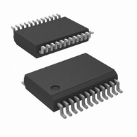
ADC12H034CIMSA/NOPB National Semiconductor, ADC12H034CIMSA/NOPB Datasheet - Page 32

ADC12H034CIMSA/NOPB
Manufacturer Part Number
ADC12H034CIMSA/NOPB
Description
ADC 12BIT W/S&H +SIGN 24-SSOP
Manufacturer
National Semiconductor
Datasheet
1.ADC12030CIWMNOPB.pdf
(42 pages)
Specifications of ADC12H034CIMSA/NOPB
Number Of Bits
12
Data Interface
NSC MICROWIRE™, Serial
Number Of Converters
4
Power Dissipation (max)
33mW
Voltage Supply Source
Analog and Digital
Operating Temperature
-40°C ~ 85°C
Mounting Type
Surface Mount
Package / Case
24-SSOP (0.200", 5.30mm Width)
Number Of Elements
1
Architecture
SAR
Input Polarity
Unipolar
Input Type
Voltage
Rated Input Volt
5V
Differential Input
Yes
Power Supply Requirement
Analog and Digital
Single Supply Voltage (typ)
5V
Single Supply Voltage (min)
4.5V
Single Supply Voltage (max)
5.5V
Dual Supply Voltage (typ)
Not RequiredV
Dual Supply Voltage (min)
Not RequiredV
Dual Supply Voltage (max)
Not RequiredV
Power Dissipation
500mW
Differential Linearity Error
±1LSB
Integral Nonlinearity Error
±1LSB
Operating Temp Range
-40C to 85C
Operating Temperature Classification
Industrial
Mounting
Surface Mount
Pin Count
24
Package Type
SSOP
Lead Free Status / RoHS Status
Lead free / RoHS Compliant
Other names
ADC12H034CIMSA
www.national.com
For pseudo-differential signed operation, the circuit of shows
a signal AC coupled to the ADC. This gives a digital output
range of −4096 to +4095. With a 2.5V reference, 1 LSB is
equal to 610 µV. Although the ADC is not production tested
with a 2.5V reference, when V
error typically will not change more than 0.1 LSB (see the
curves in the Typical Electrical Characteristics Section). With
the ADC set to an acquisition time of 10 clock periods, the
An alternative method for biasing pseudo-differential opera-
tion is to use the +2.5V from the LM4040 to bias any amplifier
circuits driving the ADC as shown in Figure 13. The value of
the resistor pull-up biasing the LM4040-2.5 will depend upon
the current required by the op amp biasing circuitry.
In the circuit of Figure 13, some voltage range is lost since the
amplifier will not be able to swing to +5V and GND with a
single +5V supply. Using an adjustable version of the LM4041
FIGURE 12. Pseudo-Differential Biasing with the Signal Source AC Coupled Directly into the ADC
A
+
and V
D
+
are +5.0V, linearity
FIGURE 11. Single-Ended Biasing
32
input biasing resistor needs to be 600Ω or less. Notice though
that the input coupling capacitor needs to be made fairly large
to bring down the high pass corner. Increasing the acquisition
time to 34 clock periods (with a 5 MHz CCLK frequency) would
allow the 600Ω to increase to 6k, which with a 1 µF coupling
capacitor would set the high pass corner at 26 Hz. Increasing
R, to 6k would allow R
to set the full scale voltage at exactly 2.048V and a lower
grade LM4040D-2.5 to bias up everything to 2.5V as shown
in Figure 14 will allow the use of all the ADC's digital output
range of −4096 to +4095 while leaving plenty of head room
for the amplifier.
Fully differential operation is shown in Figure 15. One LSB for
this case is equal to (4.1V/4096) = 1 mV.
2
to be 2k.
1135446
1135447


