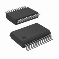
ADC12H034CIMSA/NOPB National Semiconductor, ADC12H034CIMSA/NOPB Datasheet - Page 30

ADC12H034CIMSA/NOPB
Manufacturer Part Number
ADC12H034CIMSA/NOPB
Description
ADC 12BIT W/S&H +SIGN 24-SSOP
Manufacturer
National Semiconductor
Datasheet
1.ADC12030CIWMNOPB.pdf
(42 pages)
Specifications of ADC12H034CIMSA/NOPB
Number Of Bits
12
Data Interface
NSC MICROWIRE™, Serial
Number Of Converters
4
Power Dissipation (max)
33mW
Voltage Supply Source
Analog and Digital
Operating Temperature
-40°C ~ 85°C
Mounting Type
Surface Mount
Package / Case
24-SSOP (0.200", 5.30mm Width)
Number Of Elements
1
Architecture
SAR
Input Polarity
Unipolar
Input Type
Voltage
Rated Input Volt
5V
Differential Input
Yes
Power Supply Requirement
Analog and Digital
Single Supply Voltage (typ)
5V
Single Supply Voltage (min)
4.5V
Single Supply Voltage (max)
5.5V
Dual Supply Voltage (typ)
Not RequiredV
Dual Supply Voltage (min)
Not RequiredV
Dual Supply Voltage (max)
Not RequiredV
Power Dissipation
500mW
Differential Linearity Error
±1LSB
Integral Nonlinearity Error
±1LSB
Operating Temp Range
-40C to 85C
Operating Temperature Classification
Industrial
Mounting
Surface Mount
Pin Count
24
Package Type
SSOP
Lead Free Status / RoHS Status
Lead free / RoHS Compliant
Other names
ADC12H034CIMSA
www.national.com
the start of each new conversion. Shown below is the data bit
stream required at DI, during I/O sequence number 4 in Figure
8, to set CH1 as the positive input and CH0 as the negative
input for the different versions of ADCs:
Where X can be a logic high (H) or low (L).
1.6 User Mode and Test Mode
An instruction may be issued to the ADC to put it into test
mode, which is used by the manufacturer to verify complete
functionality of the device. During test mode CH0–CH7 be-
come active outputs. If the device is inadvertently put into the
test mode with CS continuously low, the serial communica-
tions may be desynchronized. Synchronization may be re-
gained by cycling the power supply voltage to the device.
Cycling the power supply voltage will also set the device into
user mode. If CS is used in the serial interface, the ADC may
be queried to see what mode it is in. This is done by issuing
a “read STATUS register” instruction to the ADC. When bit 9
of the status register is high, the ADC is in test mode; when
bit 9 is low the ADC, is in user mode. As an alternative to
cycling the power supply, an instruction sequence may be
used to return the device to user mode. This instruction se-
quence must be issued to the ADC using CS. The following
table lists the instructions required to return the device to user
mode. Note that this entire sequence, including both Test
Mode and User Mode values, should be sent to recover from
the test mode.
ADC12H030
ADC12H032
ADC12H034
ADC12H038
ADC12030
ADC12032
ADC12034
ADC12038
Number
Part
DI0 DI1 DI2 DI3 DI4 DI5 DI6 DI7
L
L
L
L
H
H
H
H
L
L
L
L
FIGURE 8. Changing the ADC's Conversion Configuration
DI Data
L
L
L
L
H
H
L
L
H
L
L
L
H
X
X
L
X
X
X
L
30
1.5 Power Up/Down
The ADC may be powered down by taking the PD pin HIGH
or by the instruction input at DI (see Table 5 and Table 6, and
the Power Up/Down timing diagrams). When the ADC is pow-
ered down in this way, the ADC conversion circuitry is deac-
tivated but the digital I/O circuitry is kept active.
Hardware power up/down is controlled by the state of the PD
pin. Software power-up/down is controlled by the instruction
issued to the ADC. If a software power up instruction is issued
to the ADC while a hardware power down is in effect (PD pin
high) the device will remain in the power-down state. If a soft-
ware power down instruction is issued to the ADC while a
hardware power up is in effect (PD pin low), the device will
power down. When the device is powered down by software,
it may be powered up by either issuing a software power up
instruction or by taking PD pin high and then low. If the power
down command is issued during a conversion, that conver-
sion is interrupted, so the data output after power up cannot
be relied upon.
X = Don't Care
The power up, data with or without sign, and acquisition time
instructions should be resent after returning to the user mode.
This is to ensure that the ADC is in the required state before
a conversion is started.
Set DO with or
USER MODE
TEST MODE
without Sign
Instruction
Instructions
Conversion
Acquisition
Test Mode
Power Up
Start a
Reset
Time
Set
or L
or L
or L
DI0 DI1 DI2 DI3 DI4 DI5 DI6 D17
H
H
H
H
L
L
L
L
L
H or
H or
X
L
L
L
L
L
L
L
L
or L
X
H
L
L
L
L
L
L
L
H or
DI Data
X
L
L
L
L
L
L
L
L
H
H
H
H
H
H
H
H
L
or L
H
H
H
H
H
H
L
L
L
1135437
H or
H
H
H
H
H
H
H
L
L
H or
H
H
H
H
L
L
L
L
L


