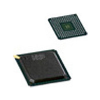
PNX1302EH NXP Semiconductors, PNX1302EH Datasheet - Page 287

PNX1302EH
Manufacturer Part Number
PNX1302EH
Description
Manufacturer
NXP Semiconductors
Datasheet
1.PNX1302EH.pdf
(548 pages)
Specifications of PNX1302EH
Lead Free Status / RoHS Status
Not Compliant
Available stocks
Company
Part Number
Manufacturer
Quantity
Price
Company:
Part Number:
PNX1302EH
Manufacturer:
NXP
Quantity:
201
Part Number:
PNX1302EH
Manufacturer:
PHILIPS/飞利浦
Quantity:
20 000
Company:
Part Number:
PNX1302EH,557
Manufacturer:
NXP Semiconductors
Quantity:
10 000
Company:
Part Number:
PNX1302EH/G
Manufacturer:
NXP
Quantity:
5 510
Part Number:
PNX1302EH/G
Manufacturer:
NXP/恩智浦
Quantity:
20 000
- Current page: 287 of 548
- Download datasheet (6Mb)
Philips Semiconductors
chip enable. If more than one device is to be added, an
external decoder, such as a 74FCT138, can be used to
decode the upper bits of the 24-bit transfer address, with
the PCI_INTB# line used as a global chip enable to the
decoder.
The PCI-XIO Bus controller has a wait state generator to
provide timing for slow devices. The wait state generator
allows the addition of up to 7 wait states for slow chip ac-
cess and write times. The wait state generator logic gen-
erates the PCI_TRDY# signal to the PCI bus.
The XIO Bus controller contains a clock generator for
standalone systems. The PCI-XIO Bus uses the PCI
clock. This clock is normally supplied by a PCI Bus cen-
tral resource outside the PNX1300 chip. In standalone or
low-cost systems, the internal clock generator can be
used. The internal clock generator divides the PNX1300
highway clock by a 5-bit number in a prescaler. This al-
lows setting bus clocks from 4 MHz to 66 MHz in a 133
MHz system. The internal clock generator programming
is described in
Figure 22-2. PCI-XIO bus device CONCEPTUAL block diagram
Section 22.5, “XIO_CTL MMIO Register.”
Unit (BIU)
PCI
Bus
Interface
XIO Bus
Controller
PCI Device
PNX1300
PCI Bus
XIO Bus
22.2
Figure 22-2
PCI-XIO Bus as a slave device on the PCI Bus. The XIO
Bus Controller generates an XIO Bus, which is an 8-bit
bus with a 24-bit address. Devices attached to the XIO
Bus appear as memory locations in the 16 MB address
space of the XIO Bus.
Figure 22-3
the PCI_XIO Bus. To conserve pins, the XIO Bus Con-
troller uses the PCI I/O pins as XIO Bus pins during XIO
Bus data transfers. It reconfigures the 32 PCI address/
data pins as 8 XIO Bus data pins and 24 XIO Bus ad-
dress pins, and it reconfigures the byte enable pins as
XIO Bus timing signals. By changing the functions of the
pins during the transfer, 36 pins are saved which would
otherwise be required to drive the XIO Bus devices. By
reconfiguring the PCI pins only during the data phase of
the XIO Bus transfers, the PCI-XIO bus retains its PCI
Bus compatibility.
Figure 22-4
PCI-XIO Bus controller.
PRELIMINARY SPECIFICATION
for address & data, these use the same pins/wires
8-bit data + 24-bit addresses
BLOCK DIAGRAM
PCI
Device
shows a more detailed block diagram of the
shows an implementation block diagram of
shows a conceptual block diagram of the
x86
Device
PCI
Device
PCI-XIO External I/O Bus
ROM
PCI
Host
22-3
Related parts for PNX1302EH
Image
Part Number
Description
Manufacturer
Datasheet
Request
R
Part Number:
Description:
NXP Semiconductors designed the LPC2420/2460 microcontroller around a 16-bit/32-bitARM7TDMI-S CPU core with real-time debug interfaces that include both JTAG andembedded trace
Manufacturer:
NXP Semiconductors
Datasheet:

Part Number:
Description:
NXP Semiconductors designed the LPC2458 microcontroller around a 16-bit/32-bitARM7TDMI-S CPU core with real-time debug interfaces that include both JTAG andembedded trace
Manufacturer:
NXP Semiconductors
Datasheet:
Part Number:
Description:
NXP Semiconductors designed the LPC2468 microcontroller around a 16-bit/32-bitARM7TDMI-S CPU core with real-time debug interfaces that include both JTAG andembedded trace
Manufacturer:
NXP Semiconductors
Datasheet:
Part Number:
Description:
NXP Semiconductors designed the LPC2470 microcontroller, powered by theARM7TDMI-S core, to be a highly integrated microcontroller for a wide range ofapplications that require advanced communications and high quality graphic displays
Manufacturer:
NXP Semiconductors
Datasheet:
Part Number:
Description:
NXP Semiconductors designed the LPC2478 microcontroller, powered by theARM7TDMI-S core, to be a highly integrated microcontroller for a wide range ofapplications that require advanced communications and high quality graphic displays
Manufacturer:
NXP Semiconductors
Datasheet:
Part Number:
Description:
The Philips Semiconductors XA (eXtended Architecture) family of 16-bit single-chip microcontrollers is powerful enough to easily handle the requirements of high performance embedded applications, yet inexpensive enough to compete in the market for hi
Manufacturer:
NXP Semiconductors
Datasheet:
Part Number:
Description:
The XA-S3 device is a member of Philips Semiconductors? XA(eXtended Architecture) family of high performance 16-bitsingle-chip microcontrollers
Manufacturer:
NXP Semiconductors
Datasheet:

Part Number:
Description:
The NXP BlueStreak LH75401/LH75411 family consists of two low-cost 16/32-bit System-on-Chip (SoC) devices
Manufacturer:
NXP Semiconductors
Datasheet:

Part Number:
Description:
The NXP LPC3130/3131 combine an 180 MHz ARM926EJ-S CPU core, high-speed USB2
Manufacturer:
NXP Semiconductors
Datasheet:

Part Number:
Description:
The NXP LPC3141 combine a 270 MHz ARM926EJ-S CPU core, High-speed USB 2
Manufacturer:
NXP Semiconductors

Part Number:
Description:
The NXP LPC3143 combine a 270 MHz ARM926EJ-S CPU core, High-speed USB 2
Manufacturer:
NXP Semiconductors

Part Number:
Description:
The NXP LPC3152 combines an 180 MHz ARM926EJ-S CPU core, High-speed USB 2
Manufacturer:
NXP Semiconductors

Part Number:
Description:
The NXP LPC3154 combines an 180 MHz ARM926EJ-S CPU core, High-speed USB 2
Manufacturer:
NXP Semiconductors

Part Number:
Description:
Standard level N-channel enhancement mode Field-Effect Transistor (FET) in a plastic package using NXP High-Performance Automotive (HPA) TrenchMOS technology
Manufacturer:
NXP Semiconductors
Datasheet:


