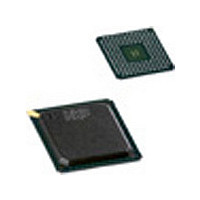
PNX1311EH NXP Semiconductors, PNX1311EH Datasheet - Page 152

PNX1311EH
Manufacturer Part Number
PNX1311EH
Description
Manufacturer
NXP Semiconductors
Datasheet
1.PNX1311EH.pdf
(548 pages)
Specifications of PNX1311EH
Lead Free Status / RoHS Status
Not Compliant
Available stocks
Company
Part Number
Manufacturer
Quantity
Price
Company:
Part Number:
PNX1311EH
Manufacturer:
NANYA
Quantity:
5 000
- Current page: 152 of 548
- Download datasheet (6Mb)
PNX1300/01/02/11 Data Book
9.9
Figure
tion of the control and status fields of the AO unit. To en-
sure compatibility with future devices, any undefined or
reserved MMIO bits should be ignored when read, and
written as zeroes
The AO unit is reset by a PNX1300 hardware reset, or by
writing 0x80000000 to the AO_CTL register. The AO unit
is not affected by DSPCPU reset initiated through the
BIU_CTL register. Either reset method sets all MMIO
fields as indicated in the tables.
The timestamp counter is reset by TRI_RESET# or by
DSPCPU reset initiated through BIU_CTL. It is not affect-
ed by AO_CTL reset. This ensures that the timestamp
9-8
Figure 9-6. AO status/control field MMIO layout.
MMIO_base
0x10 2000
0x10 2004
0x10 200C
0x10 201C
0x10 2008
0x10 2010
0x10 2014
0x10 2018
0x10 2028
0x10 2020
0x10 2024
offset:
9-6,
AUDIO OUT OPERATION
Table 9-11
AO_STATUS (r/w)
AO_CTL (r/w)
AO_SERIAL (r/w)
AO_FRAMING (r/w)
AO_FREQ (r/w)
AO_BASE1 (r/w)
AO_BASE2 (r/w)
AO_SIZE (r/w)
AO_CC (r/w)
AO_CFC (r/w)
AO_TSTAMP (r/o)
PRELIMINARY SPECIFICATION
and
SER_MASTER
TRANS_ENABLE
POLARITY
Table 9-12
DATAMODE
RESET
TRANS_MODE
CLOCK_EDGE
SIGN_CONVERT
LITTLE_ENDIAN
describe the func-
31
31
31
31
31
31
SLEEPLESS
CC1_EN
WS_PULSE
CC2_EN
SSPOS[4]
27
27
27
27
27
27
CC1
23
23
23
23
23
23
NR_CHAN
counter
CCCOUNT register.
After an AO reset, 5 AO_SCK clock cycles are required
to stabilize the internal circuitry before enabling Audio
Out. This can be accomplished by programming the
AO_FREQ and AO_SERIAL registers to start AO_SCK
generation then waiting for the appropriate 5 AO_SCK
cycle interval.
Programing of the AO_SERIAL MMIO register needs to
follow the following sequence order:
• set AO_FREQ to ensure that a valid clock is gener-
• MMIO(AO_CTL)
ated (Only when AO is the master of the audio clock
system)
BASE1
BASE2
19
19
19
19
19
19
LEFTPOS
SIZE (in samples)
FREQUENCY
TIMESTAMP
stays
15
15
15
15
15
15
CC1_POS
synchronous
RESERVED
WSDIV
UDR_INTEN
HBE (Highway bandwidth error)
= 1 << 31; /* Software Reset */
HBE_INTEN
11
11
BUF2_INTEN
11
11
11
11
BUF1_ACTIVE
Philips Semiconductors
CC_BUSY
BUF1_INTEN
RIGHTPOS
UNDERRUN
ACK_UDR
CC2
with
ACK_HBE
7
7
7
7
7
7
BUF2_EMPTY
CC2_POS
BUF1_EMPTY
0
0
0
SCKDIV
the
ACK2
0
0
0
ACK1
0
0
0
3
3
3
3
3
3
SSPOS
DSPCPU
0
0
0
0
0
0
0
0
0
0
0
0
0
0
0
Related parts for PNX1311EH
Image
Part Number
Description
Manufacturer
Datasheet
Request
R
Part Number:
Description:
NXP Semiconductors designed the LPC2420/2460 microcontroller around a 16-bit/32-bitARM7TDMI-S CPU core with real-time debug interfaces that include both JTAG andembedded trace
Manufacturer:
NXP Semiconductors
Datasheet:

Part Number:
Description:
NXP Semiconductors designed the LPC2458 microcontroller around a 16-bit/32-bitARM7TDMI-S CPU core with real-time debug interfaces that include both JTAG andembedded trace
Manufacturer:
NXP Semiconductors
Datasheet:
Part Number:
Description:
NXP Semiconductors designed the LPC2468 microcontroller around a 16-bit/32-bitARM7TDMI-S CPU core with real-time debug interfaces that include both JTAG andembedded trace
Manufacturer:
NXP Semiconductors
Datasheet:
Part Number:
Description:
NXP Semiconductors designed the LPC2470 microcontroller, powered by theARM7TDMI-S core, to be a highly integrated microcontroller for a wide range ofapplications that require advanced communications and high quality graphic displays
Manufacturer:
NXP Semiconductors
Datasheet:
Part Number:
Description:
NXP Semiconductors designed the LPC2478 microcontroller, powered by theARM7TDMI-S core, to be a highly integrated microcontroller for a wide range ofapplications that require advanced communications and high quality graphic displays
Manufacturer:
NXP Semiconductors
Datasheet:
Part Number:
Description:
The Philips Semiconductors XA (eXtended Architecture) family of 16-bit single-chip microcontrollers is powerful enough to easily handle the requirements of high performance embedded applications, yet inexpensive enough to compete in the market for hi
Manufacturer:
NXP Semiconductors
Datasheet:
Part Number:
Description:
The XA-S3 device is a member of Philips Semiconductors? XA(eXtended Architecture) family of high performance 16-bitsingle-chip microcontrollers
Manufacturer:
NXP Semiconductors
Datasheet:

Part Number:
Description:
The NXP BlueStreak LH75401/LH75411 family consists of two low-cost 16/32-bit System-on-Chip (SoC) devices
Manufacturer:
NXP Semiconductors
Datasheet:

Part Number:
Description:
The NXP LPC3130/3131 combine an 180 MHz ARM926EJ-S CPU core, high-speed USB2
Manufacturer:
NXP Semiconductors
Datasheet:

Part Number:
Description:
The NXP LPC3141 combine a 270 MHz ARM926EJ-S CPU core, High-speed USB 2
Manufacturer:
NXP Semiconductors

Part Number:
Description:
The NXP LPC3143 combine a 270 MHz ARM926EJ-S CPU core, High-speed USB 2
Manufacturer:
NXP Semiconductors

Part Number:
Description:
The NXP LPC3152 combines an 180 MHz ARM926EJ-S CPU core, High-speed USB 2
Manufacturer:
NXP Semiconductors

Part Number:
Description:
The NXP LPC3154 combines an 180 MHz ARM926EJ-S CPU core, High-speed USB 2
Manufacturer:
NXP Semiconductors

Part Number:
Description:
Standard level N-channel enhancement mode Field-Effect Transistor (FET) in a plastic package using NXP High-Performance Automotive (HPA) TrenchMOS technology
Manufacturer:
NXP Semiconductors
Datasheet:


