HUF75333S3ST Fairchild Semiconductor, HUF75333S3ST Datasheet
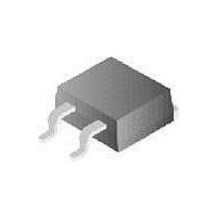
MOSFET N-CH 55V 60A D2PAK

HUF75333S3ST

Manufacturer Part Number
HUF75333S3ST
Description
MOSFET N-CH 55V 60A D2PAK
Manufacturer
Fairchild Semiconductor
Series
UltraFET™r
Datasheet

Specifications of HUF75333S3ST

Fet Type
MOSFET N-Channel, Metal Oxide
Fet Feature
Standard
Rds On (max) @ Id, Vgs
16 mOhm @ 66A, 10V
Drain To Source Voltage (vdss)
55V
Current - Continuous Drain (id) @ 25° C
60A
Vgs(th) (max) @ Id
4V @ 250µA
Gate Charge (qg) @ Vgs
85nC @ 20V
Input Capacitance (ciss) @ Vds
1300pF @ 25V
Power - Max
150W
Mounting Type
Surface Mount
Package / Case
D²Pak, TO-263 (2 leads + tab)
Configuration
Single
Transistor Polarity
N-Channel
Resistance Drain-source Rds (on)
0.016 Ohms
Drain-source Breakdown Voltage
55 V
Gate-source Breakdown Voltage
+/- 20 V
Continuous Drain Current
66 A
Power Dissipation
150 W
Maximum Operating Temperature
+ 175 C
Mounting Style
SMD/SMT
Minimum Operating Temperature
- 55 C
Lead Free Status / RoHS Status
Lead free / RoHS Compliant

Available stocks

Company
Part Number
Manufacturer
Quantity
Price
Part Number:
HUF75333S3ST
Manufacturer:
HARRIS
Quantity:
20 000
Company:
Part Number:
HUF75333S3ST
Quantity:
50 000
©2003 Fairchild Semiconductor Corporation
66A, 55V, 0.016 Ohm. N-Channel UltraFET
Power MOSFETs
achieves the lowest possible on-resistance per silicon area,
resulting in outstanding performance. This device is capable
of withstanding high energy in the avalanche mode and the
diode exhibits very low reverse recovery time and stored
charge. It was designed for use in applications where power
efficiency is important, such as switching regulators,
switching convertors, motor drivers, relay drivers, low-
voltage bus switches, and power management in portable
and battery-operated products. .
Ordering Information
NOTE: When ordering, use the entire part number. Add the suffix T to
obtain the TO-263AB variant in tape and reel, e.g., HUF75333S3ST.
Packaging
All Fairchild semiconductor products are manufactured, assembled and tested under ISO9000 and QS9000 quality systems certification.
HUF75333G3
HUF75333P3
HUF75333S3S
HUF75333S3
PART NUMBER
DRAIN
(TAB)
Product reliability information can be found at http://www.fairchildsemi.com/products/discrete/reliability/index.html
SOURCE
GATE
JEDEC STYLE TO-247
TO-247
TO-220AB
TO-263AB
TO-262AA
JEDEC TO-263AB
These N-Channel power MOSFETs
are manufactured using the
innovative UltraFET® process. This
advanced process technology
PACKAGE
Data Sheet
For severe environments, see our Automotive HUFA series.
(FLANGE)
SOURCE
DRAIN
75333G
75333P
75333S
75333S
DRAIN
HUF75333G3, HUF75333P3, HUF75333S3S,
BRAND
GATE
Features
• 66A, 55V
• Simulation Models
• Peak Current vs Pulse Width Curve
• UIS Rating Curve
• Related Literature
Formerly developmental type TA75333
Symbol
- Temperature Compensated PSPICE® and SABER™
- SPICE and SABER Thermal Impedance Models
- TB334, “Guidelines for Soldering Surface Mount
Models
Available on the WEB at: www.fairchildsemi.com
Components to PC Boards”
December 2001
(FLANGE)
(FLANGE)
DRAIN
DRAIN
HUF75333G3, HUF75333P3, HUF75333S3S, HUF75333S3 Rev. B1
JEDEC TO-262ABA
JEDEC TO-220AB
G
D
S
HUF75333S3
SOURCE
DRAIN
GATE
SOURCE
DRAIN
GATE

Related parts for HUF75333S3ST

HUF75333S3ST Summary of contents

Page 1

... HUF75333G3 TO-247 HUF75333P3 TO-220AB HUF75333S3S TO-263AB HUF75333S3 TO-262AA NOTE: When ordering, use the entire part number. Add the suffix T to obtain the TO-263AB variant in tape and reel, e.g., HUF75333S3ST. Packaging JEDEC STYLE TO-247 DRAIN (TAB) JEDEC TO-263AB GATE (FLANGE) SOURCE Product reliability information can be found at http://www.fairchildsemi.com/products/discrete/reliability/index.html For severe environments, see our Automotive HUFA series ...

Page 2

... Turn-On Delay Time Rise Time Turn-Off Delay Time Fall Time Turn-Off Time GATE CHARGE SPECIFICATIONS Total Gate Charge Gate Charge at 10V Threshold Gate Charge Gate to Source Gate Charge Gate to Drain “Miller” Charge ©2003 Fairchild Semiconductor Corporation Unless Otherwise Specified C DSS DGR ...

Page 3

... FIGURE 1. NORMALIZED POWER DISSIPATION vs CASE TEMPERATURE 2 DUTY CYCLE - DESCENDING ORDER 0.5 1 0.2 0.1 0.05 0.02 0.01 0.1 SINGLE PULSE 0. FIGURE 3. NORMALIZED MAXIMUM TRANSIENT THERMAL IMPEDANCE ©2003 Fairchild Semiconductor Corporation o C, Unless Otherwise Specified SYMBOL TEST CONDITIONS 25V 0V, ISS 1MHz C OSS (Figure 12) C RSS SYMBOL ...

Page 4

... DRAIN TO SOURCE VOLTAGE (V) DS FIGURE 5. FORWARD BIAS SAFE OPERATING AREA 150 120 PULSE DURATION = 80 s DUTY CYCLE = 0.5% MAX 1.5 3 DRAIN TO SOURCE VOLTAGE (V) DS FIGURE 7. SATURATION CHARACTERISTICS ©2003 Fairchild Semiconductor Corporation (Continued PULSE WIDTH (s) FIGURE 4. PEAK CURRENT CAPABILITY T = MAX RATED 100 s 1ms 10ms 100 200 NOTE: Refer to Fairchild Application Notes AN9321 and AN9322 ...

Page 5

... T , JUNCTION TEMPERATURE ( J FIGURE 11. NORMALIZED DRAIN TO SOURCE BREAKDOWN VOLTAGE vs JUNCTION TEMPERATURE NOTE: Refer to Fairchild Application Notes AN7254 and AN7260. FIGURE 13. GATE CHARGE WAVEFORMS FOR CONSTANT GATE CURRENT ©2003 Fairchild Semiconductor Corporation (Continued) 80 120 160 200 o C) FIGURE 10. NORMALIZED GATE THRESHOLD VOLTAGE vs 80 ...

Page 6

... Test Circuits and Waveforms VARY t TO OBTAIN P R REQUIRED PEAK FIGURE 14. UNCLAMPED ENERGY TEST CIRCUIT G(REF) FIGURE 16. GATE CHARGE TEST CIRCUIT FIGURE 18. SWITCHING TIME TEST CIRCUIT ©2003 Fairchild Semiconductor Corporation DUT 0. DUT g(REF DUT DSS FIGURE 15. UNCLAMPED ENERGY WAVEFORMS Q g(TOT) ...

Page 7

... S2BMOD VSWITCH (RON = 1e-5 ROFF = 0.1 VON = 0.5 VOFF= 0) .ENDS NOTE: For further discussion of the PSPICE model, consult A New PSPICE Sub-Circuit for the Power MOSFET Featuring Global Temperature Options; IEEE Power Electronics Specialist Conference Records, 1991, written by William J. Hepp and C. Frank Wheatley. ©2003 Fairchild Semiconductor Corporation DPLCAP 10 RSLC2 ...

Page 8

... Fairchild Semiconductor Corporation DPLCAP 10 RSLC2 - 6 ESG 8 EVTHRES + ...

Page 9

... Fairchild Semiconductor Corporation JUNCTION th RTHERM1 CTHERM1 6 RTHERM2 CTHERM2 5 RTHERM3 CTHERM3 4 RTHERM4 CTHERM4 3 RTHERM5 ...

Page 10

CROSSVOLT â â â â â Rev. I2 ...

Related keywords