A000048 Arduino, A000048 Datasheet - Page 77
A000048
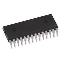
Manufacturer Part Number
A000048
Description
ATMEGA328 MCU IC W/ Arduino UNO Bootloader
Manufacturer
Arduino
Series
-r
Specifications of A000048
Accessory Type
Pre-Programed IC
Features
Powered Via USB Connection, AC-to-DC Adapter, Power Jack, ICSP Header
Core Processor
AVR
Core Size
8-Bit
Speed
20MHz
Connectivity
I²C, SPI, UART/USART
Peripherals
Brown-out Detect/Reset, POR, PWM, WDT
Number Of I /o
23
Program Memory Size
32KB (16K x 16)
Program Memory Type
FLASH
Eeprom Size
1K x 8
Ram Size
2K x 8
Voltage - Supply (vcc/vdd)
1.8 V ~ 5.5 V
Data Converters
A/D 8x10b
Oscillator Type
Internal
Operating Temperature
-40°C ~ 85°C
Package / Case
-
For Use With
ATmega328 Microcontrollers
Lead Free Status / RoHS Status
Lead free / RoHS Compliant
Lead Free Status / RoHS Status
Lead free / RoHS Compliant


13.2
13.2.1
8271C–AVR–08/10
Ports as General Digital I/O
Configuring the Pin
Note that enabling the alternate function of some of the port pins does not affect the use of the
other pins in the port as general digital I/O.
The ports are bi-directional I/O ports with optional internal pull-ups.
tional description of one I/O-port pin, here generically called Pxn.
Figure 13-2. General Digital I/O
Note:
Each port pin consists of three register bits: DDxn, PORTxn, and PINxn. As shown in
Description” on page
at the PORTx I/O address, and the PINxn bits at the PINx I/O address.
The DDxn bit in the DDRx Register selects the direction of this pin. If DDxn is written logic one,
Pxn is configured as an output pin. If DDxn is written logic zero, Pxn is configured as an input
pin.
If PORTxn is written logic one when the pin is configured as an input pin, the pull-up resistor is
activated. To switch the pull-up resistor off, PORTxn has to be written logic zero or the pin has to
be configured as an output pin. The port pins are tri-stated when reset condition becomes active,
even if no clocks are running.
ATmega48A/48PA/88A/88PA/168A/168PA/328/328
Pxn
1. WRx, WPx, WDx, RRx, RPx, and RDx are common to all pins within the same port. clk
SLEEP, and PUD are common to all ports.
PUD:
SLEEP:
clk
I/O
:
93, the DDxn bits are accessed at the DDRx I/O address, the PORTxn bits
PULLUP DISABLE
SLEEP CONTROL
I/O CLOCK
(1)
SLEEP
SYNCHRONIZER
WDx:
RDx:
WRx:
RRx:
RPx:
D
L
WPx:
Q
Q
D
PINxn
WRITE DDRx
READ DDRx
WRITE PORTx
READ PORTx REGISTER
READ PORTx PIN
WRITE PINx REGISTER
Q
Q
RESET
RESET
PORTxn
Q
Q
Q
Q
DDxn
CLR
CLR
D
D
RRx
Figure 13-2
PUD
WDx
RDx
RPx
clk
1
0
WRx
I/O
WPx
shows a func-
”Register
I/O
,
77
Related parts for A000048
Image
Part Number
Description
Manufacturer
Datasheet
Request
R

Part Number:
Description:
Daughter Cards & OEM Boards ARDUINO UNO PROTO PCB REV 3
Manufacturer:
Arduino
Part Number:
Description:
Daughter Cards & OEM Boards ARDUINO SHIELD PROTO KIT REV 3
Manufacturer:
Arduino
Part Number:
Description:
Daughter Cards & OEM Boards ARDUINO MEGA PROTO KIT REV 3
Manufacturer:
Arduino
Part Number:
Description:
Daughter Cards & OEM Boards ARDUINO MEGA PROTO PCB REV 3
Manufacturer:
Arduino
Part Number:
Description:
Development Boards & Kits - AVR ARDUINO STARTER KIT W/ UNO REV3
Manufacturer:
Arduino
Part Number:
Description:
RF Development Tools ARDUINO SHIELD WIRELESS PROTO
Manufacturer:
Arduino
Datasheet:
Part Number:
Description:
RF Development Tools ARDUINO SHIELD WIRELESS WITH SD
Manufacturer:
Arduino
Datasheet:

Part Number:
Description:
Development Software Getting started w/Arduino
Manufacturer:
Arduino

Part Number:
Description:
Ethernet Modules & Development Tools Ethernet Shield for Arduino
Manufacturer:
Arduino

Part Number:
Description:
MCU, MPU & DSP Development Tools LilyPad Arduino Main Board
Manufacturer:
Arduino

Part Number:
Description:
ARDUINO NANO Board
Manufacturer:
Arduino
Datasheet:
Part Number:
Description:
Ethernet Modules & Development Tools ETHERNET SHEILD PoE FOR ARDUINO
Manufacturer:
Arduino
Datasheet:
Part Number:
Description:
KIT XBEE/SHIELD ARDUINO
Manufacturer:
Arduino
Datasheet:
Part Number:
Description:
Memory Cards MICRO SD CARD 1GB WITH SD ADAPTER
Manufacturer:
Arduino