A000048 Arduino, A000048 Datasheet - Page 74
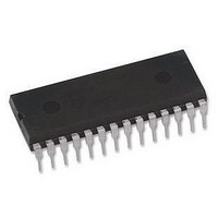
A000048
Manufacturer Part Number
A000048
Description
ATMEGA328 MCU IC W/ Arduino UNO Bootloader
Manufacturer
Arduino
Series
-r
Specifications of A000048
Accessory Type
Pre-Programed IC
Features
Powered Via USB Connection, AC-to-DC Adapter, Power Jack, ICSP Header
Core Processor
AVR
Core Size
8-Bit
Speed
20MHz
Connectivity
I²C, SPI, UART/USART
Peripherals
Brown-out Detect/Reset, POR, PWM, WDT
Number Of I /o
23
Program Memory Size
32KB (16K x 16)
Program Memory Type
FLASH
Eeprom Size
1K x 8
Ram Size
2K x 8
Voltage - Supply (vcc/vdd)
1.8 V ~ 5.5 V
Data Converters
A/D 8x10b
Oscillator Type
Internal
Operating Temperature
-40°C ~ 85°C
Package / Case
-
For Use With
ATmega328 Microcontrollers
Lead Free Status / RoHS Status
Lead free / RoHS Compliant
Lead Free Status / RoHS Status
Lead free / RoHS Compliant


12.2.4
12.2.5
8271C–AVR–08/10
PCICR – Pin Change Interrupt Control Register
PCIFR – Pin Change Interrupt Flag Register
• Bit 7:3 – Reserved
These bits are unused bits in the ATmega48A/48PA/88A/88PA/168A/168PA/328/328P, and will
always read as zero.
• Bit 2 – PCIE2: Pin Change Interrupt Enable 2
When the PCIE2 bit is set (one) and the I-bit in the Status Register (SREG) is set (one), pin
change interrupt 2 is enabled. Any change on any enabled PCINT[23:16] pin will cause an inter-
rupt. The corresponding interrupt of Pin Change Interrupt Request is executed from the PCI2
Interrupt Vector. PCINT[23:16] pins are enabled individually by the PCMSK2 Register.
• Bit 1 – PCIE1: Pin Change Interrupt Enable 1
When the PCIE1 bit is set (one) and the I-bit in the Status Register (SREG) is set (one), pin
change interrupt 1 is enabled. Any change on any enabled PCINT[14:8] pin will cause an inter-
rupt. The corresponding interrupt of Pin Change Interrupt Request is executed from the PCI1
Interrupt Vector. PCINT[14:8] pins are enabled individually by the PCMSK1 Register.
• Bit 0 – PCIE0: Pin Change Interrupt Enable 0
When the PCIE0 bit is set (one) and the I-bit in the Status Register (SREG) is set (one), pin
change interrupt 0 is enabled. Any change on any enabled PCINT[7:0] pin will cause an inter-
rupt. The corresponding interrupt of Pin Change Interrupt Request is executed from the PCI0
Interrupt Vector. PCINT[7:0] pins are enabled individually by the PCMSK0 Register.
• Bit 7:3 – Reserved
These bits are unused bits in the ATmega48A/48PA/88A/88PA/168A/168PA/328/328P, and will
always read as zero.
• Bit 2 – PCIF2: Pin Change Interrupt Flag 2
When a logic change on any PCINT[23:16] pin triggers an interrupt request, PCIF2 becomes set
(one). If the I-bit in SREG and the PCIE2 bit in PCICR are set (one), the MCU will jump to the
corresponding Interrupt Vector. The flag is cleared when the interrupt routine is executed. Alter-
natively, the flag can be cleared by writing a logical one to it.
• Bit 1 – PCIF1: Pin Change Interrupt Flag 1
When a logic change on any PCINT[14:8] pin triggers an interrupt request, PCIF1 becomes set
(one). If the I-bit in SREG and the PCIE1 bit in PCICR are set (one), the MCU will jump to the
corresponding Interrupt Vector. The flag is cleared when the interrupt routine is executed. Alter-
natively, the flag can be cleared by writing a logical one to it.
ATmega48A/48PA/88A/88PA/168A/168PA/328/328
Bit
(0x68)
Read/Write
Initial Value
Bit
0x1B (0x3B)
Read/Write
Initial Value
7
–
R
0
7
–
R
0
R
R
6
–
0
6
–
0
R
R
5
–
0
5
–
0
R
R
4
–
0
4
–
0
3
–
R
0
3
–
R
0
PCIE2
PCIF2
R/W
R/W
2
0
2
0
PCIE1
PCIF1
R/W
R/W
1
0
1
0
PCIE0
PCIF0
R/W
R/W
0
0
0
0
PCICR
PCIFR
74
Related parts for A000048
Image
Part Number
Description
Manufacturer
Datasheet
Request
R

Part Number:
Description:
Daughter Cards & OEM Boards ARDUINO UNO PROTO PCB REV 3
Manufacturer:
Arduino
Part Number:
Description:
Daughter Cards & OEM Boards ARDUINO SHIELD PROTO KIT REV 3
Manufacturer:
Arduino
Part Number:
Description:
Daughter Cards & OEM Boards ARDUINO MEGA PROTO KIT REV 3
Manufacturer:
Arduino
Part Number:
Description:
Daughter Cards & OEM Boards ARDUINO MEGA PROTO PCB REV 3
Manufacturer:
Arduino
Part Number:
Description:
Development Boards & Kits - AVR ARDUINO STARTER KIT W/ UNO REV3
Manufacturer:
Arduino
Part Number:
Description:
RF Development Tools ARDUINO SHIELD WIRELESS PROTO
Manufacturer:
Arduino
Datasheet:
Part Number:
Description:
RF Development Tools ARDUINO SHIELD WIRELESS WITH SD
Manufacturer:
Arduino
Datasheet:

Part Number:
Description:
Development Software Getting started w/Arduino
Manufacturer:
Arduino

Part Number:
Description:
Ethernet Modules & Development Tools Ethernet Shield for Arduino
Manufacturer:
Arduino

Part Number:
Description:
MCU, MPU & DSP Development Tools LilyPad Arduino Main Board
Manufacturer:
Arduino

Part Number:
Description:
ARDUINO NANO Board
Manufacturer:
Arduino
Datasheet:
Part Number:
Description:
Ethernet Modules & Development Tools ETHERNET SHEILD PoE FOR ARDUINO
Manufacturer:
Arduino
Datasheet:
Part Number:
Description:
KIT XBEE/SHIELD ARDUINO
Manufacturer:
Arduino
Datasheet:
Part Number:
Description:
Memory Cards MICRO SD CARD 1GB WITH SD ADAPTER
Manufacturer:
Arduino