A000048 Arduino, A000048 Datasheet - Page 311
A000048
Manufacturer Part Number
A000048
Description
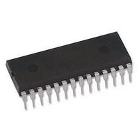
ATMEGA328 MCU IC W/ Arduino UNO Bootloader
Manufacturer
Arduino
Series
-r
Specifications of A000048
Accessory Type
Pre-Programed IC
Features
Powered Via USB Connection, AC-to-DC Adapter, Power Jack, ICSP Header
Core Processor
AVR
Core Size
8-Bit
Speed
20MHz
Connectivity
I²C, SPI, UART/USART
Peripherals
Brown-out Detect/Reset, POR, PWM, WDT
Number Of I /o
23
Program Memory Size
32KB (16K x 16)
Program Memory Type
FLASH
Eeprom Size
1K x 8
Ram Size
2K x 8
Voltage - Supply (vcc/vdd)
1.8 V ~ 5.5 V
Data Converters
A/D 8x10b
Oscillator Type
Internal
Operating Temperature
-40°C ~ 85°C
Package / Case
-
For Use With
ATmega328 Microcontrollers
Lead Free Status / RoHS Status
Lead free / RoHS Compliant
Lead Free Status / RoHS Status
Lead free / RoHS Compliant


27.7.15
27.8
8271C–AVR–08/10
Serial Downloading
Parallel Programming Characteristics
For characteristics of the Parallel Programming, see
page
Both the Flash and EEPROM memory arrays can be programmed using the serial SPI bus while
RESET is pulled to GND. The serial interface consists of pins SCK, MOSI (input) and MISO (out-
put). After RESET is set low, the Programming Enable instruction needs to be executed first
before program/erase operations can be executed. NOTE, in
mapping for SPI programming is listed. Not all parts use the SPI pins dedicated for the internal
SPI interface.
Figure 27-7. Serial Programming and Verify
Notes:
When programming the EEPROM, an auto-erase cycle is built into the self-timed programming
operation (in the Serial mode ONLY) and there is no need to first execute the Chip Erase
instruction. The Chip Erase operation turns the content of every memory location in both the
Program and EEPROM arrays into 0xFF.
Depending on CKSEL Fuses, a valid clock must be present. The minimum low and high periods
for the serial clock (SCK) input are defined as follows:
Low: > 2 CPU clock cycles for f
High: > 2 CPU clock cycles for f
ATmega48A/48PA/88A/88PA/168A/168PA/328/328
329.
1. If the device is clocked by the internal Oscillator, it is no need to connect a clock source to the
2. V
XTAL1 pin.
CC
- 0.3V <
AV
CC
< V
MOSI
MISO
SCK
ck
ck
CC
< 12 MHz, 3 CPU clock cycles for f
< 12 MHz, 3 CPU clock cycles for f
+ 0.3V, however,
XTAL1
RESET
GND
(1)
AV
CC
”Parallel Programming Characteristics” on
AVCC
VCC
should always be within 1.8 - 5.5V
+1.8 - 5.5V
+1.8 - 5.5V
Table 27-17 on page
(2)
ck
ck
>= 12 MHz
>= 12 MHz
312, the pin
311
Related parts for A000048
Image
Part Number
Description
Manufacturer
Datasheet
Request
R

Part Number:
Description:
Daughter Cards & OEM Boards ARDUINO UNO PROTO PCB REV 3
Manufacturer:
Arduino
Part Number:
Description:
Daughter Cards & OEM Boards ARDUINO SHIELD PROTO KIT REV 3
Manufacturer:
Arduino
Part Number:
Description:
Daughter Cards & OEM Boards ARDUINO MEGA PROTO KIT REV 3
Manufacturer:
Arduino
Part Number:
Description:
Daughter Cards & OEM Boards ARDUINO MEGA PROTO PCB REV 3
Manufacturer:
Arduino
Part Number:
Description:
Development Boards & Kits - AVR ARDUINO STARTER KIT W/ UNO REV3
Manufacturer:
Arduino
Part Number:
Description:
RF Development Tools ARDUINO SHIELD WIRELESS PROTO
Manufacturer:
Arduino
Datasheet:
Part Number:
Description:
RF Development Tools ARDUINO SHIELD WIRELESS WITH SD
Manufacturer:
Arduino
Datasheet:

Part Number:
Description:
Development Software Getting started w/Arduino
Manufacturer:
Arduino

Part Number:
Description:
Ethernet Modules & Development Tools Ethernet Shield for Arduino
Manufacturer:
Arduino

Part Number:
Description:
MCU, MPU & DSP Development Tools LilyPad Arduino Main Board
Manufacturer:
Arduino

Part Number:
Description:
ARDUINO NANO Board
Manufacturer:
Arduino
Datasheet:
Part Number:
Description:
Ethernet Modules & Development Tools ETHERNET SHEILD PoE FOR ARDUINO
Manufacturer:
Arduino
Datasheet:
Part Number:
Description:
KIT XBEE/SHIELD ARDUINO
Manufacturer:
Arduino
Datasheet:
Part Number:
Description:
Memory Cards MICRO SD CARD 1GB WITH SD ADAPTER
Manufacturer:
Arduino