A000048 Arduino, A000048 Datasheet - Page 305
A000048
Manufacturer Part Number
A000048
Description
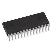
ATMEGA328 MCU IC W/ Arduino UNO Bootloader
Manufacturer
Arduino
Series
-r
Specifications of A000048
Accessory Type
Pre-Programed IC
Features
Powered Via USB Connection, AC-to-DC Adapter, Power Jack, ICSP Header
Core Processor
AVR
Core Size
8-Bit
Speed
20MHz
Connectivity
I²C, SPI, UART/USART
Peripherals
Brown-out Detect/Reset, POR, PWM, WDT
Number Of I /o
23
Program Memory Size
32KB (16K x 16)
Program Memory Type
FLASH
Eeprom Size
1K x 8
Ram Size
2K x 8
Voltage - Supply (vcc/vdd)
1.8 V ~ 5.5 V
Data Converters
A/D 8x10b
Oscillator Type
Internal
Operating Temperature
-40°C ~ 85°C
Package / Case
-
For Use With
ATmega328 Microcontrollers
Lead Free Status / RoHS Status
Lead free / RoHS Compliant
Lead Free Status / RoHS Status
Lead free / RoHS Compliant


27.7.3
27.7.4
8271C–AVR–08/10
Chip Erase
Programming the Flash
The Chip Erase will erase the Flash and EEPROM
not reset until the program memory has been completely erased. The Fuse bits are not
changed. A Chip Erase must be performed before the Flash and/or EEPROM are
reprogrammed.
Note:
Load Command “Chip Erase”
1. Set XA1, XA0 to “10”. This enables command loading.
2. Set BS1 to “0”.
3. Set DATA to “1000 0000”. This is the command for Chip Erase.
4. Give XTAL1 a positive pulse. This loads the command.
5. Give WR a negative pulse. This starts the Chip Erase. RDY/BSY goes low.
6. Wait until RDY/BSY goes high before loading a new command.
The Flash is organized in pages, see
the program data is latched into a page buffer. This allows one page of program data to be pro-
grammed simultaneously. The following procedure describes how to program the entire Flash
memory:
A. Load Command “Write Flash”
1. Set XA1, XA0 to “10”. This enables command loading.
2. Set BS1 to “0”.
3. Set DATA to “0001 0000”. This is the command for Write Flash.
4. Give XTAL1 a positive pulse. This loads the command.
B. Load Address Low byte
1. Set XA1, XA0 to “00”. This enables address loading.
2. Set BS1 to “0”. This selects low address.
3. Set DATA = Address low byte (0x00 - 0xFF).
4. Give XTAL1 a positive pulse. This loads the address low byte.
C. Load Data Low Byte
1. Set XA1, XA0 to “01”. This enables data loading.
2. Set DATA = Data low byte (0x00 - 0xFF).
3. Give XTAL1 a positive pulse. This loads the data byte.
D. Load Data High Byte
1. Set BS1 to “1”. This selects high data byte.
2. Set XA1, XA0 to “01”. This enables data loading.
3. Set DATA = Data high byte (0x00 - 0xFF).
4. Give XTAL1 a positive pulse. This loads the data byte.
E. Latch Data
1. Set BS1 to “1”. This selects high data byte.
2. Give PAGEL a positive pulse. This latches the data bytes. (See
F. Repeat B through E until the entire buffer is filled or until all data within the page is loaded.
ATmega48A/48PA/88A/88PA/168A/168PA/328/328
waveforms)
1. The EEPRPOM memory is preserved during Chip Erase if the EESAVE Fuse is programmed.
Table 27-11 on page
(1)
memories plus Lock bits. The Lock bits are
301. When programming the Flash,
Figure 27-3
for signal
305
Related parts for A000048
Image
Part Number
Description
Manufacturer
Datasheet
Request
R

Part Number:
Description:
Daughter Cards & OEM Boards ARDUINO UNO PROTO PCB REV 3
Manufacturer:
Arduino
Part Number:
Description:
Daughter Cards & OEM Boards ARDUINO SHIELD PROTO KIT REV 3
Manufacturer:
Arduino
Part Number:
Description:
Daughter Cards & OEM Boards ARDUINO MEGA PROTO KIT REV 3
Manufacturer:
Arduino
Part Number:
Description:
Daughter Cards & OEM Boards ARDUINO MEGA PROTO PCB REV 3
Manufacturer:
Arduino
Part Number:
Description:
Development Boards & Kits - AVR ARDUINO STARTER KIT W/ UNO REV3
Manufacturer:
Arduino
Part Number:
Description:
RF Development Tools ARDUINO SHIELD WIRELESS PROTO
Manufacturer:
Arduino
Datasheet:
Part Number:
Description:
RF Development Tools ARDUINO SHIELD WIRELESS WITH SD
Manufacturer:
Arduino
Datasheet:

Part Number:
Description:
Development Software Getting started w/Arduino
Manufacturer:
Arduino

Part Number:
Description:
Ethernet Modules & Development Tools Ethernet Shield for Arduino
Manufacturer:
Arduino

Part Number:
Description:
MCU, MPU & DSP Development Tools LilyPad Arduino Main Board
Manufacturer:
Arduino

Part Number:
Description:
ARDUINO NANO Board
Manufacturer:
Arduino
Datasheet:
Part Number:
Description:
Ethernet Modules & Development Tools ETHERNET SHEILD PoE FOR ARDUINO
Manufacturer:
Arduino
Datasheet:
Part Number:
Description:
KIT XBEE/SHIELD ARDUINO
Manufacturer:
Arduino
Datasheet:
Part Number:
Description:
Memory Cards MICRO SD CARD 1GB WITH SD ADAPTER
Manufacturer:
Arduino