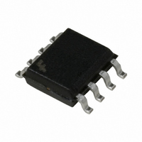
FDS3992 Fairchild Semiconductor, FDS3992 Datasheet - Page 2

FDS3992
Manufacturer Part Number
FDS3992
Description
MOSFET N-CH DUAL 100V 4.5A SO-8
Manufacturer
Fairchild Semiconductor
Series
PowerTrench®r
Type
Power MOSFETr
Datasheet
1.FDS3992.pdf
(11 pages)
Specifications of FDS3992
Fet Type
2 N-Channel (Dual)
Fet Feature
Standard
Rds On (max) @ Id, Vgs
62 mOhm @ 4.5A, 10V
Drain To Source Voltage (vdss)
100V
Current - Continuous Drain (id) @ 25° C
4.5A
Vgs(th) (max) @ Id
4V @ 250µA
Gate Charge (qg) @ Vgs
15nC @ 10V
Input Capacitance (ciss) @ Vds
750pF @ 25V
Power - Max
2.5W
Mounting Type
Surface Mount
Package / Case
8-SOIC (3.9mm Width)
Configuration
Dual Dual Drain
Transistor Polarity
N-Channel
Resistance Drain-source Rds (on)
0.062 Ohm @ 10 V
Drain-source Breakdown Voltage
100 V
Gate-source Breakdown Voltage
+/- 20 V
Continuous Drain Current
4.5 A
Power Dissipation
2500 mW
Maximum Operating Temperature
+ 150 C
Mounting Style
SMD/SMT
Minimum Operating Temperature
- 55 C
Number Of Elements
2
Polarity
N
Channel Mode
Enhancement
Drain-source On-res
0.062Ohm
Drain-source On-volt
100V
Gate-source Voltage (max)
±20V
Operating Temp Range
-55C to 150C
Operating Temperature Classification
Military
Mounting
Surface Mount
Pin Count
8
Package Type
SOIC N
Lead Free Status / RoHS Status
Lead free / RoHS Compliant
Other names
FDS3992
FDS3992TR
FDS3992TR
Available stocks
Company
Part Number
Manufacturer
Quantity
Price
Part Number:
FDS3992
Manufacturer:
FAIRCHILD/仙童
Quantity:
20 000
Part Number:
FDS3992-NL
Manufacturer:
FAIRCHILD/仙童
Quantity:
20 000
Company:
Part Number:
FDS3992_NL
Manufacturer:
FAIRCHILD
Quantity:
2 500
Part Number:
FDS3992_NL
Manufacturer:
FAIRCHILD/仙童
Quantity:
20 000
©2004 Fairchild Semiconductor Corporation
Electrical Characteristics
Off Characteristics
On Characteristics
Dynamic Characteristics
Switching Characteristics
Drain-Source Diode Characteristics
Notes:
1: Starting T
2: R
3: R
B
I
I
V
r
C
C
C
Q
Q
Q
Q
Q
t
t
t
t
t
t
V
t
Q
DSS
GSS
ON
d(ON)
r
d(OFF)
f
OFF
rr
DS(ON)
GS(TH)
VDSS
SD
ISS
OSS
RSS
g(TOT)
g(TH)
gs
gs2
gd
RR
drain pins. R
Symbol
θJA
θJA
is the sum of the junction-to-case and case-to-ambient thermal resistance where the case thermal reference is defined as the solder mounting surface of the
is measured with 1.0 in
J
= 25°C, L = 37mH, I
θJC
Drain to Source Breakdown Voltage
Zero Gate Voltage Drain Current
Gate to Source Leakage Current
Gate to Source Threshold Voltage
Drain to Source On Resistance
Input Capacitance
Output Capacitance
Reverse Transfer Capacitance
Total Gate Charge at 10V
Threshold Gate Charge
Gate to Source Gate Charge
Gate Charge Threshold to Plateau
Gate to Drain “Miller” Charge
Turn-On Time
Turn-On Delay Time
Rise Time
Turn-Off Delay Time
Fall Time
Turn-Off Time
Source to Drain Diode Voltage
Reverse Recovery Time
Reverse Recovery Charge
is guaranteed by design while R
2
copper on FR-4 board
AS
= 3A.
Parameter
(V
GS
θCA
= 10V)
T
A
is determined by the user’s board design.
= 25°C unless otherwise noted
I
V
V
V
V
I
I
I
T
V
f = 1MHz
V
V
V
V
I
I
I
I
D
D
D
D
SD
SD
SD
SD
GS
GS
C
GS
GS
DS
GS
DS
DD
GS
= 250µA, V
= 4.5A, V
= 2A, V
= 4.5A, V
= 4.5A, dI
= 4.5A, dI
= 150
= 4.5A
= 2A
= 80V
= 0V
= ±20V
= 25V, V
= 0V to 10V
= 0V to 2V
= V
= 50V, I
= 10V, R
Test Conditions
DS
o
GS
C
, I
GS
D
GS
D
SD
SD
= 6V
GS
GS
GS
= 4.5A
= 250µA
= 10V
/dt= 100A/µs
/dt= 100A/µs
= 10V,
= 0V,
= 0V
= 27Ω
T
V
I
I
D
g
C
DD
= 1.0mA
= 4.5A
= 150
= 50V
o
C
Min
100
2
-
-
-
-
-
-
-
-
-
-
-
-
-
-
-
-
-
-
-
-
-
-
-
-
0.054
0.072
0.107
750
118
Typ
1.4
3.5
2.1
2.8
27
11
23
28
26
8
-
-
-
-
-
-
-
-
-
-
-
0.062
0.108
0.123
±100
Max
1.25
250
1.9
1.0
15
47
81
48
65
1
4
-
-
-
-
-
-
-
-
-
-
-
FDS3992 Rev. B1
Units
nA
nC
nC
nC
nC
nC
µA
pF
pF
pF
nC
ns
ns
ns
ns
ns
ns
ns
V
V
V
V
Ω


