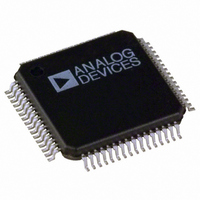
ADE7569ASTZF16-RL Analog Devices Inc, ADE7569ASTZF16-RL Datasheet - Page 92

ADE7569ASTZF16-RL
Manufacturer Part Number
ADE7569ASTZF16-RL
Description
IC,Power Metering,QFP,64PIN,PLASTIC
Manufacturer
Analog Devices Inc
Specifications of ADE7569ASTZF16-RL
Applications
Energy Measurement
Core Processor
8052
Program Memory Type
FLASH (16 kB)
Controller Series
ADE75xx
Ram Size
512 x 8
Interface
I²C, SPI, UART
Number Of I /o
20
Voltage - Supply
3.135 V ~ 3.465 V
Operating Temperature
-40°C ~ 85°C
Mounting Type
Surface Mount
Package / Case
64-LQFP
Lead Free Status / RoHS Status
Lead free / RoHS Compliant
Available stocks
Company
Part Number
Manufacturer
Quantity
Price
Company:
Part Number:
ADE7569ASTZF16-RL
Manufacturer:
Analog Devices Inc
Quantity:
10 000
ADE7566/ADE7569
VOLTAGE GENERATION
The ADE7566/ADE7569 provide two ways to generate the LCD
waveform voltage levels. The on-chip charge pump option can
generate 5 V. This makes it possible to use 5 V LCDs with the
3.3 V ADE7566/ADE7569. There is also an option to use an
external resistor ladder with a 3.3 V LCD. The EXTRES bit in
the LCD Configuration X SFR (LCDCONX, 0x9C) selects the
resistor ladder or charge pump option.
When selecting how to generate the LCD waveform voltages,
the following should be considered:
•
•
Lifetime Performance Power Consumption
In most LCDs, a high amount of current is required when the LCD
waveforms change state. The external resistor ladder option draws a
constant amount of current, whereas the charge pump circuitry
allows dynamic current consumption. If the LCD module is used
with the internal charge pump option when the display is disabled,
the voltage generation is disabled, so that no power is consumed by
the LCD function. This feature results in significant power
savings if the display is turned off during battery operation.
Contrast Control
The electrical characteristics of the liquid in the LCD change
over temperature. This requires adjustments in the LCD waveform
voltages to ensure a readable display. An added benefit of the
internal charge pump voltage generation is a configurable bias
voltage that can be compensated over temperature and supply
to maintain contrast on the LCD. These compensations can be
performed based on the ADE7566/ADE7569 temperature and
supply voltage measurements (see the Temperature, Battery, and
Supply Voltage Measurements section). This dynamic contrast
control is not easily implemented with external resistor ladder
voltage generation.
The LCD bias voltage sets the contrast of the display when the
charge pump provides the LCD waveform voltages. The ADE7566/
ADE7569 provide 64 bias levels selected by the BIASLVL bits in
the LCD Configuration X SFR (LCDCONX, 0x9C). The voltage
level on LCDVA, LCDVB and LCDVC depend on the internal
voltage reference value (V
biasing selected as described in Table 76.
Lifetime Performance
DC offset on a segment degrades its performance over time.
The voltages generated through the internal charge pump
switch faster than those generated by the external resistor
ladder, reducing the likelihood of a dc voltage being applied
to a segment and increasing the lifetime of the LCD.
LCD EXTERNAL CIRCUITRY
The voltage generation selection is made by bit EXTRES in the
LCD Configuration X SFR (LCDCONX, 0x9C). This bit is
Lifetime performance power consumption
Contrast control
REF
), BIASLVL[5:0] selection, and the
Rev. PrA | Page 92 of 136
cleared by default for charge pump voltage generation, but can
be set to enable an external resistor ladder.
Charge Pump
Voltage generation through the charge pump requires external
capacitors to store charge. The external connections to LCDVA,
LCDVB, and LCDVC, as well as LCDVP1 and LCDVP2, are
shown in Figure 76.
External Resistor Ladder
To enable the external resistor ladder option, set the EXTRES
bit in the LCD Configuration X SFR (LCDCONX, 0x9C). When
EXTRES = 1, the LCD waveform voltages are supplied by the
external resistor ladder. Because the LCD voltages are not being
generated on-chip, the LCD bias compensation implemented to
maintain contrast over temperature and supply is not possible.
The external circuitry needed for the resistor ladder option is
shown in Figure 77. The resistors required should be in the
range of 10 kΩ to 100 kΩ and based on the current required by
the LCD being used.
LCD FUNCTION IN PSM2
The LCDPSM2 and LCDEN bits in the LCD Configuration SFR
(LCDCON, 0x95) control LCD functionality in the PSM2
operating mode (see Table 86).
Table 86.
LCDPSM2
0
0
1
Note that the LCD configuration and data memory is retained
when the display is turned off.
Example LCD Setup
An example to set up the LCD peripheral for a specific LCD is
described in this section with the following parameters:
•
•
•
LCD WAVEFORM
CHARGE PUMP
Type of LCD: 5 V, 4× multiplexed with 1/3 bias, 96 segment
Voltage generation: internal charge pump
Refresh rate: 64 Hz
Figure 77. External Circuitry for External Resistor Ladder Option
CIRCUITRY
AND
Figure 76. External Circuitry for Charge Pump Option
LCD WAVEFORM
LCDEN
0
1
X
CIRCUITRY
LCDVP1
LCDVP2
Preliminary Technical Data
LCDVC
LCDVB
LCDVA
Result
The display is off in PSM2.
The display is on in PSM2.
The display is off in PSM2.
100nF
LCDVP1
LCDVP2
LCDVC
LCDVB
LCDVA
470nF
470nF
470nF


