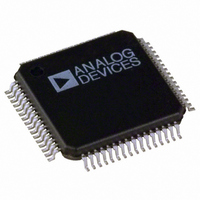
ADE7569ASTZF16-RL Analog Devices Inc, ADE7569ASTZF16-RL Datasheet - Page 41

ADE7569ASTZF16-RL
Manufacturer Part Number
ADE7569ASTZF16-RL
Description
IC,Power Metering,QFP,64PIN,PLASTIC
Manufacturer
Analog Devices Inc
Specifications of ADE7569ASTZF16-RL
Applications
Energy Measurement
Core Processor
8052
Program Memory Type
FLASH (16 kB)
Controller Series
ADE75xx
Ram Size
512 x 8
Interface
I²C, SPI, UART
Number Of I /o
20
Voltage - Supply
3.135 V ~ 3.465 V
Operating Temperature
-40°C ~ 85°C
Mounting Type
Surface Mount
Package / Case
64-LQFP
Lead Free Status / RoHS Status
Lead free / RoHS Compliant
Available stocks
Company
Part Number
Manufacturer
Quantity
Price
Company:
Part Number:
ADE7569ASTZF16-RL
Manufacturer:
Analog Devices Inc
Quantity:
10 000
Preliminary Technical Data
Table 41. Interrupt Enable Register 3 SFR (MIRQENH, 0xDB)
Bit No.
7 to 6
5
4
3
2
1
0
ANALOG INPUTS
The ADE7566/ADE7569 has two fully differential voltage input
channels. The maximum differential input voltage for input pairs
V
on analog inputs for V
AGND.
Each analog input channel has a programmable gain amplifier
(PGA) with possible gain selections of 1, 2, 4, 8, and 16. The
gain selections are made by writing to the GAIN register in the
Energy Measurement Register List (see Table 35 and Figure 31).
Bit 0 to Bit 2 select the gain for the PGA in the current channel,
and Bit 5 to Bit 7 select the gain for the PGA in the voltage
channel. Figure 30 shows how a gain selection for the current
channel is made using the gain register.
In addition to the PGA, Channel 1 also has a full-scale input
range selection for the ADC. The gain register also selects the
ADC analog input range (see Figure 31). As mentioned
previously, the maximum differential input voltage is 0.5 V.
P
/V
N
and I
WFSM
PKI
PKV
CYCEND
ZXTO
ZX
Interrupt Enable Bit
–
P
/I
N
is ±0.5 V. In addition, the maximum signal level
P
/V
N
and I
P
/I
N
is ± 0.5 V with respect to
Description
Reserved
When this bit is set, the WFSM flag set creates a pending ADE interrupt to the 8052 core.
When this bit is set, the PKI flag set creates a pending ADE interrupt to the 8052 core.
When this bit is set, the PKV flag set creates a pending ADE interrupt to the 8052 core.
When this bit is set, the CYCEND flag set creates a pending ADE interrupt to the 8052 core.
When this bit is set, the ZXTO flag set creates a pending ADE interrupt to the 8052 core.
When this bit is set, the ZX flag set creates a pending ADE interrupt to the 8052 core.
Rev. PrA | Page 41 of 136
PGA 2 GAIN SELECT
000 = × 1
001 = × 2
010 = × 4
011 = × 8
100 = × 16
*REGISTER CONTENTS SHOW POWER-ON DEFAULTS.
CURRENT AND VOLTAGE CHANNELS PGA CONTROL
V
V
V
IN
P
N
1
1
Figure 30. PGA in Current Channel
7
0
Figure 31. Analog Gain Register
7
0
6
0
6
0
GAIN REGISTER*
5
0
5
GAIN[7:0]
0
K × V
4
0
4
0
3
0
IN
3
0
2
0
CFSIGN_OPT
RESERVED
ADE7566/ADE7569
2
0
1
0
1
0
GAIN (K)
SELECTION
0
0
PGA 1 GAIN SELECT
000 = × 1
001 = × 2
010 = × 4
011 = × 8
100 = × 16
0
0
ADDR:
0x1B


