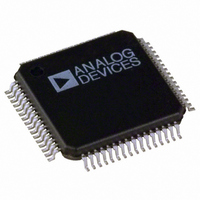
ADE7569ASTZF16-RL Analog Devices Inc, ADE7569ASTZF16-RL Datasheet - Page 102

ADE7569ASTZF16-RL
Manufacturer Part Number
ADE7569ASTZF16-RL
Description
IC,Power Metering,QFP,64PIN,PLASTIC
Manufacturer
Analog Devices Inc
Specifications of ADE7569ASTZF16-RL
Applications
Energy Measurement
Core Processor
8052
Program Memory Type
FLASH (16 kB)
Controller Series
ADE75xx
Ram Size
512 x 8
Interface
I²C, SPI, UART
Number Of I /o
20
Voltage - Supply
3.135 V ~ 3.465 V
Operating Temperature
-40°C ~ 85°C
Mounting Type
Surface Mount
Package / Case
64-LQFP
Lead Free Status / RoHS Status
Lead free / RoHS Compliant
Available stocks
Company
Part Number
Manufacturer
Quantity
Price
Company:
Part Number:
ADE7569ASTZF16-RL
Manufacturer:
Analog Devices Inc
Quantity:
10 000
ADE7566/ADE7569
Table 102. Timer 0 High Byte SFR (TH0, 0x8C)
Bit No.
7 to 0
Table 103. Timer 0 Low Byte SFR (TL0, 0x8A)
Bit No.
7 to 0
Table 104. Timer 1 High Byte SFR (TH1, 0x8D)
Bit No.
7 to 0
Table 105. Timer 1 Low Byte SFR (TL1, 0x8B)
Bit No.
7 to 0
Table 106. Timer 2 High Byte SFR (TH2, 0xCD)
Bit No.
7 to 0
Table 107. Timer 2 Low Byte SFR (TL2, 0xCC)
Bit No.
7 to 0
Table 108. Timer 2 Reload/Capture High Byte SFR
(RACP2H, 0xCB)
Bit No.
7 to 0
Table 109. Timer 2 Reload/Capture Low Byte SFR
(RACP2L, 0xCA)
Bit No.
7 to 0
TIMER 0 AND TIMER 1
Timer/Counter 0 and Timer/Counter 1 Data Registers
Each timer consists of two 8-bit registers. They are Timer 0
High Byte SFR (TH0, 0x8C), Timer 0 Low Byte SFR (TL0,
0x8A), Timer 1 High Byte SFR (TH1, 0x8D) and Timer 1 Low
Byte SFR (TL1, 0x8B) These can be used as independent
registers or combined into a single 16-bit register, depending on
the timer mode configuration (see Table 102 to Table 105).
Mnemonic
TH0
Mnemonic
TL0
Mnemonic
TH1
Mnemonic
TL1
Mnemonic
TH2
Mnemonic
TL2
Mnemonic
TH2
Mnemonic
TL2
Default
0
Default
0
Default
0
Default
0
Default
0
Default
0
Default
0
Default
0
Description
Timer 0 Data High Byte.
Description
Timer 0 Data High Byte.
Description
Timer 1 Data High Byte.
Description
Timer 1 Data High Byte.
Description
Timer 2 Data High Byte.
Description
Timer 2 Data High Byte.
Description
Timer 2 Reload/
Capture High Byte.
Description
Timer 2 Reload/
Capture Low Byte.
Rev. PrA | Page 102 of 136
Timer/Counter 0 and Timer/Counter 1 Operating Modes
This section describes the operating modes for Timer/Counter 0
and Timer/Counter 1. Unless otherwise noted, these modes of
operation are the same for both Timer 0 and Timer 1.
Mode 0 (13-Bit Timer/Counter)
Mode 0 configures an 8-bit timer/counter. Figure 82 shows
Mode 0 operation. Note that the divide-by-12 prescaler is not
present on the single-cycle core.
In this mode, the timer register is configured as a 13-bit register.
As the count rolls over from all 1s to all 0s, it sets the timer
overflow flag, TF0. TF0 can then be used to request an interrupt.
The counted input is enabled to the timer when TR0 = 1 and either
Gate = 0 or INT0 = 1. Setting Gate0 = 1 allows the timer to be
controlled by external input INT0 to facilitate pulse-width
measurements. TR0 is a control bit in the Timer/Counter 0 and
Timer/Counter 1 Control SFR (TCON, 0x88); the Gate bit is in
Timer/Counter 0 and Timer/Counter 1 Mode SFR (TMOD,
0x89). The 13-bit register consists of all 8 bits of Timer 0 High
Byte SFR (TH0, 0x8C) and the lower 5 bits of Timer 0 Low Byte
SFR (TL0, 0x8A). The upper 3 bits of Timer 0 Low Byte SFR
(TL0, 0x8A) are indeterminate and should be ignored. Setting
the run flag (TR0) does not clear the registers.
Mode 1 (16-Bit Timer/Counter)
Mode 1 is the same as Mode 0 except that the Mode 1 timer
register runs with all 16 bits. Mode 1 is shown in Figure 83.
f
P0.6/T0
P0.6/T0
f
CORE
GATE
CORE
GATE
I
INT
NT0
0
TR0
TR0
Figure 82. Timer/Counter 0, Mode 0
Figure 83. Timer/Counter 0, Mode 1
C/T0 = 0
C/T0 = 1
C/T0 = 0
C/T0 = 1
Preliminary Technical Data
CONTROL
CONTROL
(8 BITS)
(5 BITS)
TL0
TL0
(8 BITS)
(8 BITS)
TH0
TH0
TF0
TF0
INTERRUPT
INTERRUPT


