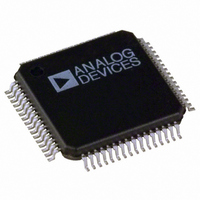
ADE7569ASTZF16-RL Analog Devices Inc, ADE7569ASTZF16-RL Datasheet - Page 122

ADE7569ASTZF16-RL
Manufacturer Part Number
ADE7569ASTZF16-RL
Description
IC,Power Metering,QFP,64PIN,PLASTIC
Manufacturer
Analog Devices Inc
Specifications of ADE7569ASTZF16-RL
Applications
Energy Measurement
Core Processor
8052
Program Memory Type
FLASH (16 kB)
Controller Series
ADE75xx
Ram Size
512 x 8
Interface
I²C, SPI, UART
Number Of I /o
20
Voltage - Supply
3.135 V ~ 3.465 V
Operating Temperature
-40°C ~ 85°C
Mounting Type
Surface Mount
Package / Case
64-LQFP
Lead Free Status / RoHS Status
Lead free / RoHS Compliant
Available stocks
Company
Part Number
Manufacturer
Quantity
Price
Company:
Part Number:
ADE7569ASTZF16-RL
Manufacturer:
Analog Devices Inc
Quantity:
10 000
ADE7566/ADE7569
Table 138. SPI Interrupt Status Register SFR (SPISTAT, 0xEA)
Bit No.
7
6
5
4
3
2
1
0
SPI PINS
MISO (Master in, Slave out Data I/O Pin)
The MISO pin is configured as an input line in master mode
and as an output line in slave mode. The MISO line on the
master (data in) should be connected to the MISO line in the
slave device (data out). The data is transferred as byte-wide
(8-bit) serial data, MSB first.
MOSI (Master out, Slave in Pin)
The MOSI pin is configured as an output line in master mode
and as an input line in slave mode. The MOSI line on the master
(data out) should be connected to the MOSI line in the slave
device (data in).The data is transferred as byte-wide (8-bit)
serial data, MSB first.
Mnemonic
BUSY
MMERR
SPIRxOF
SPIRxIRQ
SPIRxBF
SPITxUF
SPITxIRQ
SPITxBF
Default
0
0
0
0
0
0
0
0
Description
SPI Peripheral Busy Flag.
BUSY
0
1
SPI Multi-Master Error Flag.
MMERR
0
1
SPI Receive Overflow Error Flag. Reading the SPI2CRx SFR clears this bit.
SPIRxOF
0
1
SPI Receive Mode Interrupt Flag. Reading the SPI2CRx SFR clears this bit.
SPIRxIRQ
0
1
1
Status Bit for SPI Rx Buffer. When set, the Rx FIFO is full. A read of the SPI2CRx clears this flag
Status Bit for SPI Tx Buffer. When set, the Tx FIFO is underflowing and data can be written into SPI2CTx.
Write a 0 to this bit to clear it.
SPI Transmit Mode Interrupt Flag. Writing new data to the SPI2CTx SFR clears this bit.
SPITxIRQ
0
1
1
Status Bit for SPI Tx Buffer. When set, the SPI Tx buffer is full. Write a 0 to this bit to clear it.
Result
The SPI peripheral is idle.
The SPI peripheral is busy transferring data in slave or master mode.
Result
A multiple master error has not occurred.
If the SS_EN bit is set, enabling the slave select input and asserting the SS while the SPI
peripheral is transferring data as a master, this flag is raised to indicate the error.
Write a 0 to this bit to clear it.
TIMODE
X
1
TIMODE
X
0
1
TIMODE
X
0
1
Rev. PrA | Page 122 of 136
Result
The SPI2CRx register contains valid data
This bit is set if the SPI2CRx register is not read before the end of the next byte
transfer. If the RxOFW bit is set and this condition occurs, SPI2CRx is overwritten.
Result
The SPI2CRx register does not contain new data.
This bit is set when the SPI2CRx register contains new data. If the SPI/I
interrupt is enabled, an interrupt is generated when this bit is set. If the SPI2CRx
register is not read before the end of the current byte transfer, the transfer stop
and the SS is deasserted.
The SPI2CRx register contains new data.
Result
The SPI2CTx register is full.
The SPI2CTx register is empty.
This bit is set when the SPI2CTx register is empty. If the SPI/I
enabled, an interrupt is generated when this bit is set. If new data is not written
into the SPI2CTx SFR before the end of the current byte transfer, the transfer
stops, and the SS is deasserted. Write a 0 to this bit to clear it.
SCLK (Serial Clock I/O Pin)
The master serial clock (SCLK) is used to synchronize the data
being transmitted and received through the MOSI and MISO
data lines. The SCLK pin is configured as an output in master
mode and as an input in slave mode.
In master mode, the bit rate, polarity, and phase of the clock are
controlled by the SPI Configuration Register SFR (SPIMOD1,
0xE8) and SPI Configuration Register SFR (SPIMOD2, 0xE9).
In slave mode, the SPI Configuration Register SFR (SPIMOD2,
0xE9) must be configured with the phase and polarity of the
expected input clock.
In both master and slave modes, the data is transmitted on one
edge of the SCLK signal and sampled on the other. It is important,
therefore, that the SPICPHA and SPICPOL bits are configured
the same for the master and slave devices.
Preliminary Technical Data
2
C interrupt is
2
C


