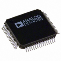
ADE7569ASTZF16-RL Analog Devices Inc, ADE7569ASTZF16-RL Datasheet - Page 56

ADE7569ASTZF16-RL
Manufacturer Part Number
ADE7569ASTZF16-RL
Description
IC,Power Metering,QFP,64PIN,PLASTIC
Manufacturer
Analog Devices Inc
Specifications of ADE7569ASTZF16-RL
Applications
Energy Measurement
Core Processor
8052
Program Memory Type
FLASH (16 kB)
Controller Series
ADE75xx
Ram Size
512 x 8
Interface
I²C, SPI, UART
Number Of I /o
20
Voltage - Supply
3.135 V ~ 3.465 V
Operating Temperature
-40°C ~ 85°C
Mounting Type
Surface Mount
Package / Case
64-LQFP
Lead Free Status / RoHS Status
Lead free / RoHS Compliant
Available stocks
Company
Part Number
Manufacturer
Quantity
Price
Company:
Part Number:
ADE7569ASTZF16-RL
Manufacturer:
Analog Devices Inc
Quantity:
10 000
ADE7566/ADE7569
Reactive Power Gain Calibration
Figure 58 shows the signal processing chain for the ADE7569
reactive power calculation. As explained in the Reactive Power
Calculation for the ADE7569 section, the reactive power is
calculated by applying a low-pass filter to the instantaneous
reactive power signal. Note that when reading the waveform
samples from the output of LPF2, the gain of the reactive
energy can be adjusted by using the multiplier and by writing
a twos complement, 12-bit word to the VAR gain register
(VARGAIN[11:0]). Equation 25 shows how the gain adjustment
is related to the contents of the watt gain register.
The resolution of the VARGAIN register is the same as the
WGAIN register (see the Active Power Gain Calibration
section). VARGAIN can be used to calibrate the reactive
power (or energy) calculation in the ADE7569.
Reactive Power Offset Calibration
The ADE7569 also incorporates a reactive power offset register
(VAROS[15:0]). This is a signed, twos complement, 16-bit register
that can be used to remove offsets in the reactive power
calculation (see Figure 58). An offset can exist in the reactive
power calculation due to crosstalk between channels on the
PCB or in the IC itself. The offset calibration allows the
contents of the reactive power register to be maintained at 0
when no power is being consumed.
The 256 LSBs (VAROS = 0x100) written to the reactive power
offset register are equivalent to 1 LSB in the WAVMODE register.
Sign of Reactive Power Calculation
Note that the average reactive power is a signed calculation.
The phase shift filter has −90° phase shift when the integrator
is enabled, and +90° phase shift when the integrator is disabled.
Table 42 summarizes the relationship of the phase difference
between the voltage and the current and the sign of the resulting
VAR calculation.
Table 42. Sign of Reactive Power Calculation
Angle
Between 0° to 90°
Between –90° to 0°
Between 0° to 90°
Between –90° to 0°
Reactive Power Sign Detection
The ADE7569 detects a change of sign in the reactive power.
The VARSIGN flag in the Interrupt Status Register 1 SFR
(MIRQSTL, 0xDC) records when a change of sign has occurred
according to VARSIGN bit in the ACCMODE Register (0x0F).
If the VARSIGN bit is set in the Interrupt Enable Register 1 SFR
(MIRQENL, 0xD9), the 8052 core has a pending ADE interrupt.
Output VARGAIN =
⎛
⎜
⎝
Reactive
Power
×
⎧ +
⎨
⎩
1
VARGAIN
Integrator
Off
Off
On
On
2
12
⎫
⎬
⎭
⎞
⎟
⎠
Sign
Positive
Negative
Positive
Negative
Rev. PrA | Page 56 of 136
(25)
The ADE interrupt stays active until the VARSIGN status bit is
cleared (see the Energy Measurement Interrupts section).
When VARSIGN in the ACCMODE Register (0x0F) is cleared
(default), the VARSIGN flag in the Interrupt Status Register 1
SFR (MIRQSTL, 0xDC) is set when a transition from positive to
negative reactive power has occurred.
When VARSIGN in the ACCMODE Register (0x0F) is set, the
VARSIGN flag in the Interrupt Status Register 1 SFR
(MIRQSTL, 0xDC) is set when a transition from negative to
positive reactive power has occurred.
Reactive Power No-Load Detection
The ADE7569 includes a no-load threshold feature on the
reactive energy that eliminates any creep effects in the meter.
The ADE7569 accomplishes this by not accumulating reactive
energy if the multiplier output is below the no-load threshold.
When the reactive power is below the no-load threshold, the
RNOLOAD flag in the Interrupt Status Register 1 SFR
(MIRQSTL, 0xDC) is set. If the RNOLOAD bit is set in the
Interrupt Enable Register 1 SFR (MIRQENL, 0xD9), the 8052
core has a pending ADE interrupt. The ADE interrupt stays
active until the RNOLOAD status bit is cleared (see the Energy
Measurement Interrupts section).
The no-load threshold level is selectable by setting the
VARNOLOAD bits in the NLMODE Register (0x0E).
Setting these bits to 0b00 disable the no-load detection,
and setting them to 0b01, 0b10, or 0b11 set the no-load
detection threshold to 0.015%, 0.0075%, and 0.0037% of
the full-scale output frequency of the multiplier, respectively.
REACTIVE ENERGY CALCULATION FOR THE
ADE7569
As for active energy, the ADE7569 achieves the integration of
the reactive power signal by continuously accumulating the
reactive power signal in an internal, nonreadable, 49-bit energy
register. The reactive energy register (VARHR[23:0]) represents
the upper 24 bits of this internal register. The VARHR register
and its function is available for the AD7569, but not for the
AD7566.
The discrete time sample period (T) for the accumulation register
in the ADE7569 is 1.22 μs (5/MCLK). As well as calculating the
energy, this integration removes any sinusoidal components
that may be in the active power signal. Figure 58 shows this
discrete time integration or accumulation. The reactive power
signal in the waveform register is continuously added to the
internal reactive energy register.
The reactive energy accumulation depends on the setting of the
SAVARM and ABSVARM bits in the ACCMODE Register (0x0F).
When both bits are cleared, the addition is signed and, therefore,
negative energy is subtracted from the reactive energy contents.
When both bits are set, the ADE7569 is set to be in the more
restrictive mode, the absolute accumulation mode.
Preliminary Technical Data


