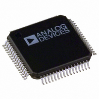
ADE7518ASTZF16-RL Analog Devices Inc, ADE7518ASTZF16-RL Datasheet - Page 121

ADE7518ASTZF16-RL
Manufacturer Part Number
ADE7518ASTZF16-RL
Description
1-Phase Energy Meter IC
Manufacturer
Analog Devices Inc
Datasheet
1.ADE7518ASTZF16.pdf
(128 pages)
Specifications of ADE7518ASTZF16-RL
Applications
Energy Measurement
Core Processor
8052
Program Memory Type
FLASH (16 kB)
Controller Series
ADE75xx
Ram Size
512 x 8
Interface
I²C, SPI, UART
Number Of I /o
20
Voltage - Supply
3.135 V ~ 3.465 V
Operating Temperature
-40°C ~ 85°C
Mounting Type
Surface Mount
Package / Case
64-LQFP
Lead Free Status / RoHS Status
Lead free / RoHS Compliant
Available stocks
Company
Part Number
Manufacturer
Quantity
Price
Company:
Part Number:
ADE7518ASTZF16-RL
Manufacturer:
Analog Devices Inc
Quantity:
10 000
I/O PORTS
PARALLEL I/O
The ADE7518 uses three input/output ports to exchange data
with external devices. In addition to performing general-purpose
I/O, some are capable of driving an LCD or performing alternate
functions for the peripherals available on-chip. In general, when a
peripheral is enabled, the pins associated with it cannot be used as
a general-purpose I/O. The I/O port can be configured through
the SFRs listed in Table 136.
Table 136. I/O Port SFRs
SFR
P0
P1
P2
EPCFG
PINMAP0
PINMAP1
PINMAP2
The three bidirectional I/O ports have internal pull-ups that can
be enabled or disabled individually for each pin. The internal
pull-ups are enabled by default. Disabling an internal pull-up
causes a pin to become open drain. Weak internal pull-ups are
configured through the PINMAPx SFRs.
Figure 101 shows a typical bit latch and I/O buffer for an I/O pin.
The bit latch (one bit in each port’s SFR) is represented as a
Type D flip-flop, which clocks in a value from the internal bus
in response to a write-to-latch signal from the CPU. The Q output
of the flip-flop is placed on the internal bus in response to a read
latch signal from the CPU. The level of the port pin itself is
placed on the internal bus in response to a read pin signal from
the CPU. Some instructions that read a port activate the read
latch signal, and others activate the read pin signal. See the
Read-Modify-Write Instructions section for details.
INTERNAL
TO LATCH
LATCH
WRITE
READ
READ
BUS
PIN
Address
0x80
0x90
0xA0
0x9F
0xB2
0xB3
0xB4
Figure 101. Port 0 Bit Latch and I/O Buffer
LATCH
CL
D
Q
Q
Bit Addressable
Yes
Yes
Yes
No
No
No
No
ALTERNATE
ALTERNATE
FUNCTION
FUNCTION
OUTPUT
INPUT
DV
DD
CLOSED: PINMAPx.x = 0
OPEN: PINMAPx.x = 1
INTERNAL
PULL-UP
Description
Port 0.
Port 1.
Port 2.
Extended Port
Configuration.
Port 0 Weak
Pull-Up Enable.
Port 1 Weak
Pull-Up Enable.
Port 2 Weak
Pull-Up Enable.
Px.x
PIN
Rev. 0 | Page 121 of 128
Weak Internal Pull-Ups Enabled
A pin with weak internal pull-up enabled is used as an input by
writing a 1 to the pin. The pin is pulled high by the internal pull-
ups, and the pin is read using the circuitry shown in Figure 101.
If the pin is driven low externally, it sources current because of
the internal pull-ups.
A pin with internal pull-up enabled is used as an output by
writing a 1 or a 0 to the pin to control the level of the output.
If a 0 is written to the pin, it drives a logic low output voltage
(V
Open Drain (Weak Internal Pull-Ups Disabled)
When the weak internal pull-up on a pin is disabled, the pin
becomes open drain. Use this open-drain pin as a high impedance
input by writing a 1 to the pin. The pin is read using the circuitry
shown in Figure 101. The open-drain option is preferable for
inputs because it draws less current than the internal pull-ups
that were enabled.
38 kHz Modulation
The ADE7518 provides a 38 kHz modulation signal. The
38 kHz modulation is accomplished by internally XOR’ing the
level written to the I/O pin with a 38 kHz square wave. Then,
when a 0 is written to the I/O pin, it is modulated as shown in
Figure 102.
Uses for this 38 kHz modulation include IR modulation of
a UART transmit signal or a low power signal to drive an
LED. The modulation can be enabled or disabled with the
MOD38EN bit in the CFG SFR. The 38 kHz modulation is
available on eight pins, selected by the MOD38[7:0] bits in
the Extended Port Configuration SFR (EPCFG, 0x9F).
OL
38kHz MODULATION
38kHz MODULATED
) and is capable of sinking 1.6 mA.
LEVEL WRITTEN
OUTPUT PIN
TO MOD38
SIGNAL
Figure 102. 38 kHz Modulation
ADE7518


