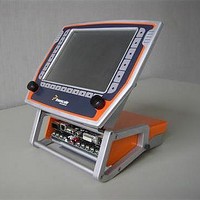
MEDIA5200KIT1 Freescale Semiconductor, MEDIA5200KIT1 Datasheet - Page 17

MEDIA5200KIT1
Manufacturer Part Number
MEDIA5200KIT1
Description
MCU, MPU & DSP Development Tools MEDIA5200 SW DEVT SYSTEM
Manufacturer
Freescale Semiconductor
Specifications of MEDIA5200KIT1
Processor To Be Evaluated
MPC5200B
Data Bus Width
32 bit
Interface Type
Ethernet, USB
Lead Free Status / Rohs Status
Not Compliant
2) The interrupt latency descriptions in the table above are related to non competitive, non masked but enabled external interrupt
Because all external interrupt signals are synchronized into the internal processor bus clock domain, each of these signals has
to exceed a minimum pulse width of more than one IP_CLK cycle.
NOTES:
1) The frequency of the IP_CLK depends on the register settings in Clock Distribution Module. See the MPC5200B User’s Manual
2) If the same interrupt occurs a second time while its interrupt service routine has not cleared the former one, the second
Besides synchronization, prioritization, and mapping the latency of an external interrupt to the start of its associated interrupt
service routine also depends on the following conditions: To get a minimum interrupt service response time, it is recommended
to enable the instruction cache and set up the maximum core clock, XL bus, and IP bus frequencies (depending on board design
and programming). In addition, it is advisable to execute an interrupt handler, which has been implemented in assembly code.
1.3.6
1.3.6.1
Freescale Semiconductor
sources. Take care of interrupt prioritization which may increase the latencies.
(MPC5200BUM) for further information.
interrupt is not recognized at all.
data
t
data
DM
DM
mem_clk
Sym
t
t
valid
hold
All external interrupts (IRQs, GPIOs)
valid
hold
setup
hold
SDRAM
Control Signals, Address and MBA Valid after
Control Signals, Address and MBA Hold after
Memory Interface Timing-Standard SDRAM Read Command
DQM valid after rising edge of MEM_CLK
DQM hold after rising edge of MEM_CLK
MDQ hold after rising edge of MEM_CLK
MDQ setup to rising edge of MEM_CLK
Table 17. Minimum Pulse Width for External Interrupts to be Recognized
Name
rising edge of MEM_CLK
rising edge of MEM_CLK
MEM_CLK period
Description
Table 18. Standard SDRAM Memory Read Timing
MPC5200B Data Sheet, Rev. 4
Min Pulse Width
> 1 clock cycle
t
mem_clk
t
mem_clk
Min
× 0.25 – 0.7
7.5
0.2
—
—
—
Max Pulse Width
× 0.5
—
t
t
mem_clk
mem_clk
Max
× 0.25 + 0.4
0.3
× 0.5 + 0.4
—
—
—
—
Reference Clock
IP_CLK
Units
ns
ns
ns
ns
ns
ns
ns
SpecID
A4.22
SpecID
A5.1
A5.2
A5.3
A5.4
A5.5
A5.6
A5.7
17


