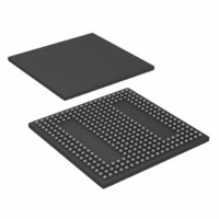
ADSP-BF538BBCZ-5F4 Analog Devices Inc, ADSP-BF538BBCZ-5F4 Datasheet - Page 27

ADSP-BF538BBCZ-5F4
Manufacturer Part Number
ADSP-BF538BBCZ-5F4
Description
IC, FLOAT-PT DSP, 16BIT, 533MHZ, BGA-316
Manufacturer
Analog Devices Inc
Series
Blackfinr
Type
Fixed Pointr
Specifications of ADSP-BF538BBCZ-5F4
No. Of Bits
16 Bit
Frequency
533MHz
Supply Voltage
1.25V
Embedded Interface Type
CAN, I2C, PPI, SPI, TWI, UART
No. Of I/o's
54
Flash Memory Size
512KB
Interface
CAN, SPI, SSP, TWI, UART
Clock Rate
533MHz
Non-volatile Memory
FLASH (512 kB)
On-chip Ram
148kB
Voltage - I/o
3.00V, 3.30V
Voltage - Core
1.25V
Operating Temperature
-40°C ~ 85°C
Mounting Type
Surface Mount
Package / Case
316-CSPBGA
Lead Free Status / RoHS Status
Lead free / RoHS Compliant
For Use With
ADZS-BFAUDIO-EZEXT - BOARD EVAL AUDIO BLACKFIN
Lead Free Status / RoHS Status
Lead free / RoHS Compliant, Lead free / RoHS Compliant
ABSOLUTE MAXIMUM RATINGS
Stresses greater than those listed below may cause permanent
damage to the device. These are stress ratings only. Functional
operation of the device at these or any other conditions greater
than those indicated in the operational sections of this specifica-
tion is not implied. Exposure to absolute maximum rating
conditions for extended periods may affect device reliability.
Table 18. Absolute Maximum Ratings
1
2
3
4
Table 19. Maximum Duty Cycle for Input Transient Voltage
1
2
3
ESD SENSITIVITY
Parameter
Internal (Core) Supply Voltage (V
External (I/O) Supply Voltage (V
Input Voltage
Input Voltage
Output Voltage Swing
Junction Temperature While Biased
Storage Temperature Range
V
–0.50
–0.70
–0.80
–0.90
–1.00
Parameter value applies also to V
Applies to 100% transient duty cycle. For other duty cycles, see
Applies only when V
Applies to pins designated as 5 V tolerant only.
Applies to all signal pins with the exception of CLKIN, XTAL, and VROUT1–0.
The individual values cannot be combined for analysis of a single instance of
Duty cycle refers to the percentage of time the signal exceeds the value for the
fications, the range is V
overshoot or undershoot. The worst case observed value must fall within one of
the voltages specified and the total duration of the overshoot or undershoot
(exceeding the 100% case) must be less than or equal to the corresponding
duty cycle.
100% case. This is equivalent to the measured duration of a single instance of
overshoot or undershoot as a percentage of the period of occurrence.
IN
Min (V)
2
2, 3
4, 4
ESD (electrostatic discharge) sensitive device.
Charged devices and circuit boards can discharge
without detection. Although this product features
patented or proprietary protection circuitry, damage
may occur on devices subjected to high energy ESD.
Therefore, proper ESD precautions should be taken to
avoid performance degradation or loss of functionality.
V
+3.80
+4.00
+4.10
+4.20
+4.30
DDEXT
IN
DDEXT
Max (V)
is within specifications. When V
± 0.2 V.
DDRTC
2
.
DDEXT
DDINT
Maximum Duty Cycle
100%
40%
25%
15%
10%
)
1
)
Rating
–0.3 V to +1.4 V
–0.3 V to +3.8 V
–0.5 V to +3.6 V
–0.5 V to +5.5 V
–0.5 V to V
+125°C
–65°C to +150°C
DDEXT
Table
DDEXT
is outside speci-
Rev. D | Page 27 of 56 | July 2010
19.
3
+ 0.5 V
1
PACKAGE INFORMATION
The information presented in
information about how to read the package brand and relate it
to specific product features. For a complete listing of product
offerings, see the
Table 20. Package Brand Information
Brand Key
t
pp
Z
ccc
vvvvvv.x
n.n
#
yyww
Figure 9. Product Information on Package
Ordering Guide on Page
ADSP-BF538/ADSP-BF538F
yyww country_of_origin
Field Description
Temperature Range
Package Type
RoHS Compliant Part
See Ordering Guide
Assembly Lot Code
Silicon Revision
RoHS Compliant Designation
Date Code
ADSP-BF538
vvvvvv.x n.n
tppZccc
Figure 9
and
56.
Table 20
provides


