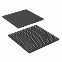
ADSP-BF538BBCZ-5F4 Analog Devices Inc, ADSP-BF538BBCZ-5F4 Datasheet - Page 19

ADSP-BF538BBCZ-5F4
Manufacturer Part Number
ADSP-BF538BBCZ-5F4
Description
IC, FLOAT-PT DSP, 16BIT, 533MHZ, BGA-316
Manufacturer
Analog Devices Inc
Series
Blackfinr
Type
Fixed Pointr
Specifications of ADSP-BF538BBCZ-5F4
No. Of Bits
16 Bit
Frequency
533MHz
Supply Voltage
1.25V
Embedded Interface Type
CAN, I2C, PPI, SPI, TWI, UART
No. Of I/o's
54
Flash Memory Size
512KB
Interface
CAN, SPI, SSP, TWI, UART
Clock Rate
533MHz
Non-volatile Memory
FLASH (512 kB)
On-chip Ram
148kB
Voltage - I/o
3.00V, 3.30V
Voltage - Core
1.25V
Operating Temperature
-40°C ~ 85°C
Mounting Type
Surface Mount
Package / Case
316-CSPBGA
Lead Free Status / RoHS Status
Lead free / RoHS Compliant
For Use With
ADZS-BFAUDIO-EZEXT - BOARD EVAL AUDIO BLACKFIN
Lead Free Status / RoHS Status
Lead free / RoHS Compliant, Lead free / RoHS Compliant
PIN DESCRIPTIONS
The ADSP-BF538/ADSP-BF538F processors pin definitions are
listed in
All pins are three-stated during and immediately after reset,
except the memory interface, asynchronous memory control,
and synchronous memory control pins. These pins are all
driven high, with the exception of CLKOUT, which toggles at
the system clock rate. If BR is active (whether or not RESET is
asserted), the memory pins are also three-stated. All unused I/O
pins have their input buffers disabled with the exception of the
Table 10. Pin Descriptions
Pin Name
Memory Interface
ADDR19–1
DATA15–0
ABE1–0/SDQM1–0
BR
BG
BGH
Asynchronous Memory Control
AMS3–0
ARDY
AOE
ARE
AWE
Flash Control
FCE
FRESET
Synchronous Memory Control
SRAS
SCAS
SWE
SCKE
CLKOUT
SA10
SMS
Timers
TMR0
TMR1/PPI_FS1
TMR2/PPI_FS2
Table
10.
I/O
O
I/O
O
I
O
O
O
I
O
O
O
I
I
O
O
O
O
O
O
O
I/O
I/O
I/O
Address Bus for Async/Sync Access
Data Bus for Async/Sync Access
Flash Enable (This pin is internally connected to GND on the ADSP-BF538.)
Function
Byte Enables/Data Masks for Async/Sync Access
Bus Request (This pin should be pulled high when not used.)
Bus Grant
Bus Grant Hang
Bank Select (Require pull-ups if hibernate is used.)
Hardware Ready Control
Output Enable
Read Enable
Write Enable
Flash Reset (This pin is internally connected to GND on the ADSP-BF538.)
Row Address Strobe
Column Address Strobe
Write Enable
Clock Enable (This pin must be pulled low through a 10 kΩ resistor if
hibernate state is used and SDRAM contents need to be preserved during
hibernate.)
Clock Output
A10 Pin
Bank Select
Timer 0
Timer 1/PPI Frame Sync1
Timer 2/PPI Frame Sync2
Rev. D | Page 19 of 56 | July 2010
pins that need pull-ups or pull-downs, as noted in the table.
During hibernate, all outputs are three-stated unless otherwise
noted in
In order to maintain maximum functionality and reduce pack-
age size and pin count, some pins have dual, multiplexed
functionality. In cases where pin functionality is reconfigurable,
the default state is shown in plain text, while alternate function-
ality is shown in italics.
Table
10.
ADSP-BF538/ADSP-BF538F
Driver Type
A
A
A
A
A
A
A
A
A
A
A
A
B
A
A
C
C
C
A
1


