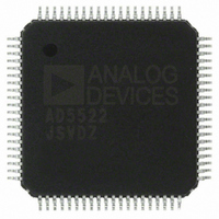
AD5522JSVDZ Analog Devices Inc, AD5522JSVDZ Datasheet - Page 9

AD5522JSVDZ
Manufacturer Part Number
AD5522JSVDZ
Description
IC, DAC, 16BIT, QFP-80
Manufacturer
Analog Devices Inc
Datasheet
1.AD5522JSVDZ.pdf
(64 pages)
Specifications of AD5522JSVDZ
Resolution (bits)
16bit
Input Channel Type
Serial
Supply Voltage Range - Digital
2.3V To 5.25V
Supply Current
36mA
Digital Ic Case Style
QFP
No. Of Pins
80
Data Interface
LVDS, Serial
Design Resources
Parametric Measurement Unit and Supporting Components for PAD Appls Using AD5522 and AD7685 (CN0104)
Lead Free Status / RoHS Status
Lead free / RoHS Compliant
Available stocks
Company
Part Number
Manufacturer
Quantity
Price
Company:
Part Number:
AD5522JSVDZ
Manufacturer:
WD
Quantity:
1 000
Company:
Part Number:
AD5522JSVDZ
Manufacturer:
Analog Devices Inc
Quantity:
10 000
Part Number:
AD5522JSVDZ
Manufacturer:
ADI/亚德诺
Quantity:
20 000
Parameter
GUARDx PIN
FORCE AMPLIFIER
FV SETTLING TIME TO 0.05% OF FS
MI SETTLING TIME TO 0.05% OF FS
FI SETTLING TIME TO 0.05% OF FS
MV SETTLING TIME TO 0.05% OF FS
DAC SPECIFICATIONS
COMPARATOR DAC DYNAMIC
REFERENCE INPUT
Output Voltage Span
Output Offset
Short-Circuit Current
Maximum Load Capacitance
Output Impedance
Tristate Leakage Current
Slew Rate
Alarm Activation Time
Slew Rate
Gain Bandwidth
Max Stable Load Capacitance
±80 mA Range
±2 mA Range
±200 μA Range
±20 μA Range
±5 μA Range
±80 mA Range
±2 mA Range
±200 μA Range
±20 μA Range
±5 μA Range
±80 mA Range
±2 mA Range
±200 μA Range
±20 μA Range
±5 μA Range
±80 mA Range
±2 mA Range
±200 μA Range
±20 μA Range
±5 μA Range
Resolution
Output Voltage Span
Differential Nonlinearity
SPECIFICATIONS
Output Voltage Settling Time
Slew Rate
Digital-to-Analog Glitch Energy
Glitch Impulse Peak Amplitude
VREF DC Input Impedance
VREF Input Current
VREF Range
2
2
2
2
2
2
2
2
2
2
2
2
2
Min
−10
−15
−30
−1
1
−10
2
Typ
22.5
85
5
200
0.4
1.3
22
24
40
300
1400
22
24
60
462
1902
24
24
50
450
2700
24
24
50
450
2700
22.5
1
5.5
20
10
100
+0.03
1
Rev. D | Page 9 of 64
Max
+10
+15
100
+30
10,000
100
40
40
80
40
40
100
55
60
120
55
60
120
16
+1
+10
5
Unit
V
mV
mA
V/μs
pF
LSB
μs
V/μs
mV
MΩ
μA
nF
Ω
nA
V/μs
μs
MHz
nF
μs
μs
μs
μs
μs
μs
μs
μs
μs
μs
μs
μs
μs
μs
μs
μs
μs
μs
μs
μs
Bits
V
nV-sec
V
Test Conditions/Comments
When guard amplifier is disabled
C
Alarm delayed to eliminate false alarms
CCOMPx = 100 pF, CFFx = 220 pF, C
CCOMPx = 100 pF, CFFx = 220 pF, C
CCOMPx = 100 pF, larger C
capacitor
CCOMPx = 1 nF, larger C
capacitor
Midscale to full-scale change; measured from
SYNC rising edge, clamps on
CCOMPx = 100 pF, CFFx = 220 pF, C
CCOMPx = 100 pF, CFFx = 220 pF, C
CCOMPx = 100 pF, CFFx = 220 pF, C
CCOMPx = 100 pF, CFFx = 220 pF, C
CCOMPx = 100 pF, CFFx = 220 pF, C
Midscale to full-scale change; driven from force
amplifier in FV mode, so includes FV settling time;
measured from SYNC rising edge, clamps on
CCOMPx = 100 pF, CFFx = 220 pF, C
CCOMPx = 100 pF, CFFx = 220 pF, C
CCOMPx = 100 pF, CFFx = 220 pF, C
CCOMPx = 100 pF, CFFx = 220 pF, C
CCOMPx = 100 pF, CFFx = 220 pF, C
Midscale to full-scale change; measured from
SYNC rising edge, clamps on
CCOMPx = 100 pF, C
CCOMPx = 100 pF, C
CCOMPx = 100 pF, C
CCOMPx = 100 pF, C
CCOMPx = 100 pF, C
Midscale to full-scale change; driven from force
amplifier in FV mode, so includes FV settling time;
measured from SYNC rising edge, clamps on
CCOMPx = 100 pF, C
CCOMPx = 100 pF, C
CCOMPx = 100 pF, C
CCOMPx = 100 pF, C
CCOMPx = 100 pF, C
VREF = 5 V, within a range of −16.25 V to +22.5 V
Guaranteed monotonic by design over temperature
500 mV change to ±½ LSB
LOAD
= 10 pF
LOAD
LOAD
LOAD
LOAD
LOAD
LOAD
LOAD
LOAD
LOAD
LOAD
LOAD
= 200 pF
= 200 pF
= 200 pF
= 200 pF
= 200 pF
= 200 pF
= 200 pF
= 200 pF
= 200 pF
= 200 pF
LOAD
requires larger CCOMP
requires larger CCOMP
LOAD
LOAD
LOAD
LOAD
LOAD
LOAD
LOAD
LOAD
LOAD
LOAD
LOAD
LOAD
AD5522
= 200 pF
= 200 pF
= 200 pF
= 200 pF
= 200 pF
= 200 pF
= 200 pF
= 200 pF
= 200 pF
= 200 pF
= 200 pF
= 200 pF


