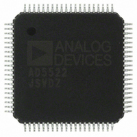
AD5522JSVDZ Analog Devices Inc, AD5522JSVDZ Datasheet - Page 12

AD5522JSVDZ
Manufacturer Part Number
AD5522JSVDZ
Description
IC, DAC, 16BIT, QFP-80
Manufacturer
Analog Devices Inc
Datasheet
1.AD5522JSVDZ.pdf
(64 pages)
Specifications of AD5522JSVDZ
Resolution (bits)
16bit
Input Channel Type
Serial
Supply Voltage Range - Digital
2.3V To 5.25V
Supply Current
36mA
Digital Ic Case Style
QFP
No. Of Pins
80
Data Interface
LVDS, Serial
Design Resources
Parametric Measurement Unit and Supporting Components for PAD Appls Using AD5522 and AD7685 (CN0104)
Lead Free Status / RoHS Status
Lead free / RoHS Compliant
Available stocks
Company
Part Number
Manufacturer
Quantity
Price
Company:
Part Number:
AD5522JSVDZ
Manufacturer:
WD
Quantity:
1 000
Company:
Part Number:
AD5522JSVDZ
Manufacturer:
Analog Devices Inc
Quantity:
10 000
Part Number:
AD5522JSVDZ
Manufacturer:
ADI/亚德诺
Quantity:
20 000
AD5522
Parameter
t
t
t
t
1
2
3
4
5
6
Table 3. LVDS Interface
Parameter
t
t
t
t
t
t
t
t
1
2
3
4
16
17
18
19
1
2
3
4
5
6
7
8
Guaranteed by design and characterization; not production tested.
All input signals are specified with t
See Figure 5 and Figure 6.
Writes to more than one X1 register engages the calibration engine for longer times, shown by the BUSY low time, t
should either be timed or should wait until BUSY returns high (see Figure 56). This is required to ensure that data is not lost or overwritten.
t
SDO output slows with lower DVCC supply and may require use of a slower SCLK.
Guaranteed by design and characterization; not production tested.
All input signals are specified with t
See Figure 7.
SDO output slows with lower DVCC supply and may require use of slower SCLK.
19
4
5, 6
is measured with the load circuit shown in Figure 4.
1, 2, 3
1, 2, 3
2.3 V to 2.7 V
1.8
670
400
60
2.7 V to 3.6 V
20
8
3
3
5
3
45
150
70
400
R
R
DVCC, Limit at T
= t
= t
DVCC, Limit at T
F
F
= 2 ns (10% to 90% of DVCC) and timed from a voltage level of 1.2 V.
= 2 ns (10% to 90% of DVCC) and timed from a voltage level of 1.2 V.
1.2
700
400
45
2.7 V to 3.6 V
4.5 V to 5.25 V
12
5
3
3
3
3
25
150
70
400
MIN
MIN
, T
, T
4.5 V to 5.25 V
0.9
750
400
25
MAX
MAX
Rev. D | Page 12 of 64
Unit
ns min
ns min
ns min
ns min
ns min
ns min
ns min
ns min
ns min
ns min
Unit
μs min
μs max
ns min
ns max
Description
SCLK cycle time
SCLK pulse width high and low time
SYNC to SCLK setup time
Data setup time
Data hold time
SCLK to SYNC hold time
SCLK rising edge to SDO valid
Minimum SYNC high time in write mode after
X1 register write
Minimum SYNC high time in write mode after
any other register write
Minimum SYNC high time in readback mode
Description
RESET pulse width low
RESET time indicated by BUSY low
Minimum SYNC high time in readback mode
SCLK rising edge to SDO valid; DVCC = 5 V to 5.25 V
10
. Subsequent writes to one or more X1 registers


