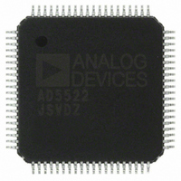
AD5522JSVDZ Analog Devices Inc, AD5522JSVDZ Datasheet - Page 11

AD5522JSVDZ
Manufacturer Part Number
AD5522JSVDZ
Description
IC, DAC, 16BIT, QFP-80
Manufacturer
Analog Devices Inc
Datasheet
1.AD5522JSVDZ.pdf
(64 pages)
Specifications of AD5522JSVDZ
Resolution (bits)
16bit
Input Channel Type
Serial
Supply Voltage Range - Digital
2.3V To 5.25V
Supply Current
36mA
Digital Ic Case Style
QFP
No. Of Pins
80
Data Interface
LVDS, Serial
Design Resources
Parametric Measurement Unit and Supporting Components for PAD Appls Using AD5522 and AD7685 (CN0104)
Lead Free Status / RoHS Status
Lead free / RoHS Compliant
Available stocks
Company
Part Number
Manufacturer
Quantity
Price
Company:
Part Number:
AD5522JSVDZ
Manufacturer:
WD
Quantity:
1 000
Company:
Part Number:
AD5522JSVDZ
Manufacturer:
Analog Devices Inc
Quantity:
10 000
Part Number:
AD5522JSVDZ
Manufacturer:
ADI/亚德诺
Quantity:
20 000
Parameter
1
2
TIMING CHARACTERISTICS
AVDD ≥ 10 V, AVSS ≤ −5 V, |AVDD − AVSS| ≥ 20 V and ≤ 33 V, DVCC = 2.3 V to 5.25 V, VREF = 5 V, T
otherwise noted.
Table 2. SPI Interface
Parameter
t
t
t
t
t
t
t
t
t
t
t
t
t
t
t
t
WRITE
1
2
3
4
5
6
7
8
9
10
11
12
13
14
15
Typical specifications are at 25°C and nominal supply, ±15.25 V, unless otherwise noted.
Guaranteed by design and characterization; not production tested. Tempco values are mean and standard deviation, unless otherwise noted.
4
Power Supply Sensitivity
1 DAC X1
2 DAC X1
3 DAC X1
4 DAC X1
Other Registers
4
ΔForced Voltage/ΔAVDD
ΔForced Voltage/ΔAVSS
ΔMeasured Current/ΔAVDD
ΔMeasured Current/ΔAVSS
ΔForced Current/ΔAVDD
ΔForced Current/ΔAVSS
ΔMeasured Voltage/ΔAVDD
ΔMeasured Voltage/ΔAVSS
ΔForced Voltage/ΔDVCC
ΔMeasured Current/ΔDVCC
ΔForced Current/ΔDVCC
ΔMeasured Voltage/ΔDVCC
1, 2, 3
2.3 V to 2.7 V
1030
950
30
8
8
10
150
70
10
5
9
120
1.65
2.3
2.95
3.6
270
20
20
150
0
100
2
DVCC, Limit at T
2.7 V to 3.6 V
735
655
20
8
8
10
150
70
5
5
7
75
1.65
2.3
2.95
3.6
270
20
20
150
0
100
Min
MIN
, T
4.5 V to 5.25 V
735
655
20
8
8
10
150
70
5
5
4.5
55
1.65
2.3
2.95
3.6
270
20
20
150
0
100
Typ
−80
−80
−85
−75
−75
−75
−85
−80
−90
−90
−90
−90
MAX
1
Rev. D | Page 11 of 64
Max
Unit
ns min
ns min
ns min
ns min
ns min
ns min
ns min
ns min
ns min
ns min
ns min
ns max
μs max
μs max
μs max
μs max
ns max
ns min
ns min
ns min
ns min
ns max
Unit
dB
dB
dB
dB
dB
dB
dB
dB
dB
dB
dB
dB
Description
Single channel update cycle time (X1 register write)
Single channel update cycle time (any other register write)
SCLK cycle time
SCLK high time
SCLK low time
SYNC falling edge to SCLK falling edge setup time
Minimum SYNC high time in write mode after X1 register
write (one channel)
Minimum SYNC high time in write mode after any
other register write
29
Data setup time
Data hold time
SYNC rising edge to BUSY falling edge
BUSY pulse width low for X1 and some PMU register writes;
see
System control register/PMU registers
29
LOAD pulse width low
BUSY rising edge to FOHx output response time
BUSY rising edge to LOAD falling edge
LOAD falling edge to FOHx output response time
th
th
Table 17
SCLK falling edge to SYNC rising edge
SCLK falling edge to LOAD falling edge
Test Conditions/Comments
From dc to 1 kHz
and
Table 18
J
= 25°C to 90°C, unless
AD5522


