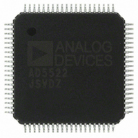
AD5522JSVDZ Analog Devices Inc, AD5522JSVDZ Datasheet - Page 49

AD5522JSVDZ
Manufacturer Part Number
AD5522JSVDZ
Description
IC, DAC, 16BIT, QFP-80
Manufacturer
Analog Devices Inc
Datasheet
1.AD5522JSVDZ.pdf
(64 pages)
Specifications of AD5522JSVDZ
Resolution (bits)
16bit
Input Channel Type
Serial
Supply Voltage Range - Digital
2.3V To 5.25V
Supply Current
36mA
Digital Ic Case Style
QFP
No. Of Pins
80
Data Interface
LVDS, Serial
Design Resources
Parametric Measurement Unit and Supporting Components for PAD Appls Using AD5522 and AD7685 (CN0104)
Lead Free Status / RoHS Status
Lead free / RoHS Compliant
Available stocks
Company
Part Number
Manufacturer
Quantity
Price
Company:
Part Number:
AD5522JSVDZ
Manufacturer:
WD
Quantity:
1 000
Company:
Part Number:
AD5522JSVDZ
Manufacturer:
Analog Devices Inc
Quantity:
10 000
Part Number:
AD5522JSVDZ
Manufacturer:
ADI/亚德诺
Quantity:
20 000
Bit
14
13
12
11
10
9
8
7
6
5
4
3
2
1
0 (LSB)
1
2
Writing 101 in Bit 17 to Bit 15 disables the always on mode for the external current range buffer. Use with FV mode (FORCE1 = FORCE0 = 0) only. To complete the
disabling of the always on mode, the PMU channel is placed into high-Z mode and the external current range buffer is returned to its default operation (off).
Writing 110 in Bit 17 to Bit 15 places the external current range buffer into always on mode. In this mode, the buffer is always active with no regard to the selected current
range. The always on mode is intended for use where an external high current stage is being used for a current drive in excess of ±80 mA; having the internal stage
always on should help to eliminate timing concerns when transitioning between this current range and other ranges. When first enabling the always on mode, use it in
conjunction with FV mode (FORCE1 = FORCE0 = 0); the device now enables the external current range buffer. The 110 code also places the device into high-Z mode
(necessary to complete the enabling function). To return to an FV or FI operating mode, select the appropriate mode and current range. The external range sense
resistor is connected to an MI circuit only when the external current range address is selected (C2 to C0 are set to 100). The default operation at power-on is disabled
(or off).
Bit Name
MEAS1
MEAS0
FIN
SF0
SS0
CL
CPOLH
Compare
V/I
Clear
Unused
Description
The MEAS1 and MEAS0 bits specify the required measure mode, allowing the MEASOUTx line to be disabled,
connected to the temperature sensor, or enabled for measurement of current or voltage.
MEAS1
0
0
1
1
This bit sets the status of the force input (FIN) amplifier.
0 = input of the force amplifier switched to GND.
1 = input of the force amplifier connected to the FIN DAC output.
The SF0 and SS0 bits specify the switching of system force and sense lines to the force and sense paths at the
DUT. The channel to which the system force and system sense lines are connected is set by the PMU3 to PMU0
bits. For correct operation, only one PMU channel should be connected to the SYS_FORCE and SYS_SENSE
paths at any one time.
SF0
0
0
1
1
Per-PMU current or voltage clamp enable bit. A logic high enables the clamp function for the selected PMU. The
clamp enable function is also available in the system control register. This dual functionality allows flexible
enabling or disabling of this function. When reading back information about the status of the clamp enable
function on a per-channel basis, the data that was most recently written to the clamp register is available in the
readback word from either the PMU register or the system control register.
Comparator output enable bit. By default, the comparator outputs are high-Z on power-on. A logic high enables
the comparator output for the selected PMU. The comparator function CPBIASEN (Bit 13 in the system control
register), must be enabled. The comparator output enable function is also available in the system control register.
This dual functionality allows flexible enabling or disabling of this function. When reading back information about
the status of the comparator enable function, the data that was most recently written to the comparator status
register is available in the readback word from either the PMU register or the system control register.
A logic high selects the compare voltage function; a logic low selects the compare current function.
To clear or reset a latched alarm bit and pin (temperature, guard, or clamp), write a 1 to this bit. This bit applies
to latched alarm conditions (clamp and guard) on all four PMU channels.
Unused bits. Set to 0.
SS0
0
1
0
1
MEAS0
0
1
0
1
Action
SYS_FORCE and SYS_SENSE are high-Z for the selected channel
SYS_FORCE is high-Z and SYS_SENSE is connected to MEASVHx for the selected channels
SYS_FORCE is connected to FOHx and SYS_SENSE is high-Z for the selected channel
SYS_FORCE is connected to FOHx and SYS_SENSE is connected to MEASVHx for the selected
channel
Rev. D | Page 49 of 64
Action
MEASOUTx is connected to I
MEASOUTx is connected to V
MEASOUTx is connected to the temperature sensor
MEASOUTx is high-Z (SW12 open)
SENSE
SENSE
AD5522


