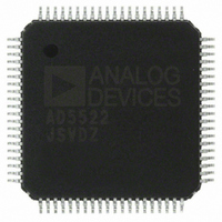
AD5522JSVDZ Analog Devices Inc, AD5522JSVDZ Datasheet - Page 50

AD5522JSVDZ
Manufacturer Part Number
AD5522JSVDZ
Description
IC, DAC, 16BIT, QFP-80
Manufacturer
Analog Devices Inc
Datasheet
1.AD5522JSVDZ.pdf
(64 pages)
Specifications of AD5522JSVDZ
Resolution (bits)
16bit
Input Channel Type
Serial
Supply Voltage Range - Digital
2.3V To 5.25V
Supply Current
36mA
Digital Ic Case Style
QFP
No. Of Pins
80
Data Interface
LVDS, Serial
Design Resources
Parametric Measurement Unit and Supporting Components for PAD Appls Using AD5522 and AD7685 (CN0104)
Lead Free Status / RoHS Status
Lead free / RoHS Compliant
Available stocks
Company
Part Number
Manufacturer
Quantity
Price
Company:
Part Number:
AD5522JSVDZ
Manufacturer:
WD
Quantity:
1 000
Company:
Part Number:
AD5522JSVDZ
Manufacturer:
Analog Devices Inc
Quantity:
10 000
Part Number:
AD5522JSVDZ
Manufacturer:
ADI/亚德诺
Quantity:
20 000
AD5522
WRITE DAC REGISTER
The DAC input, gain, and offset registers are addressed through
a combination of PMU bits (Bit 27 to Bit 24) and mode bits
(Bit 23 and Bit 22). Bit A5 to Bit A0 address each DAC level on
Table 27. DAC Register Bits
B28
RD/WR
Table 28. DAC Register Functions
Bit
28 (MSB)
27
26
25
24
23
22
DAC Register-Specific Bits
21
20
19
18
17
16
15 to 0
B27
PMU3
Bit Name
RD/WR
PMU3
PMU2
PMU1
PMU0
MODE1
MODE0
A5
A4
A3
A2
A1
A0
D15 (MSB) to
D0 (LSB)
B26
PMU2
B25
PMU1
When this bit is low, a write function takes place to the selected register; setting the RD/WR bit high initiates a
readback sequence of the PMU, alarm status, comparator status, system control, or DAC register, as determined
by the address bits.
Bit PMU3 to Bit PMU0 address each PMU and DAC channel in the device. These bits allow control of each
individual DAC channel or any combination of channels, in addition to multichannel programming.
The MODE1 and MODE0 bits allow addressing of the DAC gain (M), offset (C), or input (X1) register.
MODE1
0
0
1
1
DAC address bits. The A5 to A3 bits select the register set that is addressed. See the DAC Addressing section.
DAC address bits. The A2 to A0 bits select the DAC that is addressed. See the DAC Addressing section.
16 DAC data bits for X1 and C registers. M register is 15 bits wide, D15 to D1.
Description
B24
PMU0
B23
MODE1
MODE0
0
1
0
1
B22
MODE0
Rev. D | Page 50 of 64
Action
Write to the system control register or the PMU register
Write to the DAC gain (M) register
Write to the DAC offset (C) register
Write to the DAC input data (X1) register
B21
A5
B20
A4
chip. Bit D15 to Bit D0 are the DAC data bits used when writing
to these registers. The PMU address bits allow addressing of a
particular DAC for any combination of PMU channels.
B19
A3
B18
A2
B17
A1
B16
A0
B15 to B0
Data Bits[D15 (MSB):D0 (LSB)]


