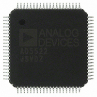
AD5522JSVDZ Analog Devices Inc, AD5522JSVDZ Datasheet - Page 30

AD5522JSVDZ
Manufacturer Part Number
AD5522JSVDZ
Description
IC, DAC, 16BIT, QFP-80
Manufacturer
Analog Devices Inc
Datasheet
1.AD5522JSVDZ.pdf
(64 pages)
Specifications of AD5522JSVDZ
Resolution (bits)
16bit
Input Channel Type
Serial
Supply Voltage Range - Digital
2.3V To 5.25V
Supply Current
36mA
Digital Ic Case Style
QFP
No. Of Pins
80
Data Interface
LVDS, Serial
Design Resources
Parametric Measurement Unit and Supporting Components for PAD Appls Using AD5522 and AD7685 (CN0104)
Lead Free Status / RoHS Status
Lead free / RoHS Compliant
Available stocks
Company
Part Number
Manufacturer
Quantity
Price
Company:
Part Number:
AD5522JSVDZ
Manufacturer:
WD
Quantity:
1 000
Company:
Part Number:
AD5522JSVDZ
Manufacturer:
Analog Devices Inc
Quantity:
10 000
Part Number:
AD5522JSVDZ
Manufacturer:
ADI/亚德诺
Quantity:
20 000
AD5522
THEORY OF OPERATION
The AD5522 is a highly integrated, quad per-pin parametric
measurement unit (PPMU) for use in semiconductor automated
test equipment. It provides programmable modes to force a pin
voltage and measure the corresponding current (FVMI) and
to force a pin current and measure the corresponding voltage
(FIMV). The device is also capable of all other combinations,
including force high-Z and measure high-Z. The PPMU can
force or measure a voltage range of 22.5 V. It can force or
measure currents up to ±80 mA per channel using the internal
amplifier; the addition of an external amplifier enables higher
current ranges. All the DAC levels required for each PMU
channel are on chip.
FORCE AMPLIFIER
The force amplifier drives the analog output, FOHx, which
drives a programmed current or voltage to the device under
test (DUT). Headroom and footroom requirements for this
amplifier are 3 V on either end. An additional ±1 V is dropped
across the sense resistor when maximum (rated) current is
flowing through it.
The force amplifier is designed to drive DUT capacitances up
to 10 nF, with a compensation value of 100 pF. Larger DUT
capacitive loads require larger compensation capacitances.
Local feedback ensures that the amplifiers are stable when
disabled. A disabled channel reduces power consumption by
2.5 mA per channel.
COMPARATORS
Per channel, the DUT measured voltage or current is monitored
by two comparators configured as window comparators. Internal
DAC levels set the CPL (comparator low) and CPH (comparator
high) threshold values. There are no restrictions on the voltage
settings of the comparator highs and lows. CPL going higher
than CPH is not a useful operation; however, it does not cause
any problems with the device. CPOLx (comparator output low)
and CPOHx (comparator output high) are continuous time
comparator outputs.
Table 8. Comparator Output Function Using SPI Interface
Test Condition
V
V
V
V
CPH > V
When using the SPI interface, full comparator functionality is
available. When using the LVDS interface, the comparator
function is limited to one output per comparator, due to the
large pin count requirement of the LVDS interface.
When using the LVDS interface, the comparator output available
pins, CPO0 to CPO3, provide information on whether the meas-
ured voltage or current is inside or outside the set CPH and CPL
DUT
DUT
DUT
DUT
or I
or I
or I
or I
DUT
DUT
DUT
DUT
DUT
> CPH
< CPH
> CPL
< CPL
or I
DUT
> CPL
CPOLx
1
0
1
CPOHx
0
1
1
Rev. D | Page 30 of 64
window. Information on whether the measurement was high or
low is available via the serial interface (comparator status register).
Table 9. Comparator Output Function Using LVDS Interface
Test Condition
(CPL < (V
(CPL > (V
CLAMPS
Current and voltage clamps are included on chip, one clamp for
each PMU channel. The clamps protect the DUT in the event of
an open-circuit or short-circuit condition. Internal DAC levels
set the CLL (clamp low) and CLH (clamp high) levels. The clamps
work to limit the force amplifier if a voltage or current at the
DUT exceeds the set levels. The clamps also protect the DUT if
a transient voltage or current spike occurs when changing to a
different operating mode or when programming the device to a
different current range.
The voltage clamps are available while forcing current, and the
current clamps are available while forcing voltage. The user can
set up the voltage or current clamp status (enabled or disabled)
using the serial interface (system control register or PMU register).
Each clamp has a smooth, finite transition region between
normal (unclamped) operation and the final clamped level, and
an internal flag is activated within this transition zone. The
open-drain CGALM pin indicates whether one or more PMU
channels has clamped. The clamp status of an individual PMU
can be determined by polling the alarm status register using the
SPI or LVDS interface.
CLL should never be greater than CLH. For the voltage clamps,
there should be 500 mV between the CLL and CLH levels to
ensure that a region exists in the middle of the clamps where
both are off. Similarly, set current clamps ±250 mV away from 0 A.
The transfer function for voltage clamping in FI mode is
See the DAC Levels section for more information.
The transfer function for current clamping in FV mode is
where:
R
MI_Amplifier_Gain is the gain of the measure current
instrumentation amplifier, either 5 or 10.
Do not change clamp levels while the channel is in force mode
because this can affect the forced voltage or current applied to
the DUT. Similarly, the clamps should not be enabled or
disabled during a force operation.
SENSE
VCLL or VCLH = 4.5 × VREF × (DAC_CODE/2
(3.5 × VREF × (OFFSET_DAC_CODE/2
ICLL or ICLH = 4.5 × VREF × ((DAC_CODE −
32,768)/2
is the sense resistor of the selected current range.
DUT
DUT
or I
or I
16
DUT
DUT
)/(R
)) and ((V
)) or ((V
SENSE
× MI_Amplifier_Gain)
DUT
DUT
or I
or I
DUT
DUT
) > CPH)
) < CPH)
16
CPOx Output
1
0
)) + DUTGND
16
) −


