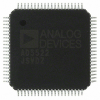
AD5522JSVDZ Analog Devices Inc, AD5522JSVDZ Datasheet - Page 10

AD5522JSVDZ
Manufacturer Part Number
AD5522JSVDZ
Description
IC, DAC, 16BIT, QFP-80
Manufacturer
Analog Devices Inc
Datasheet
1.AD5522JSVDZ.pdf
(64 pages)
Specifications of AD5522JSVDZ
Resolution (bits)
16bit
Input Channel Type
Serial
Supply Voltage Range - Digital
2.3V To 5.25V
Supply Current
36mA
Digital Ic Case Style
QFP
No. Of Pins
80
Data Interface
LVDS, Serial
Design Resources
Parametric Measurement Unit and Supporting Components for PAD Appls Using AD5522 and AD7685 (CN0104)
Lead Free Status / RoHS Status
Lead free / RoHS Compliant
Available stocks
Company
Part Number
Manufacturer
Quantity
Price
Company:
Part Number:
AD5522JSVDZ
Manufacturer:
WD
Quantity:
1 000
Company:
Part Number:
AD5522JSVDZ
Manufacturer:
Analog Devices Inc
Quantity:
10 000
Part Number:
AD5522JSVDZ
Manufacturer:
ADI/亚德诺
Quantity:
20 000
AD5522
Parameter
DIE TEMPERATURE SENSOR
INTERACTION AND CROSSTALK
SPI INTERFACE LOGIC INPUTS
CMOS LOGIC OUTPUTS
OPEN-DRAIN LOGIC OUTPUTS
LVDS INTERFACE LOGIC INPUTS
LVDS INTERFACE LOGIC OUTPUTS
POWER SUPPLIES
Accuracy
Output Voltage at 25°C
Output Scale Factor
Output Voltage Range
DC Crosstalk (FOHx)
DC Crosstalk (MEASOUTx)
DC Crosstalk Within a Channel
Input High Voltage, V
Input Low Voltage, V
Input Current, I
Input Capacitance, C
Output High Voltage, V
Output Low Voltage, V
Tristate Leakage Current
Output Capacitance
Output Low Voltage, V
Output Capacitance
REDUCED RANGE LINK
Input Voltage Range
Input Differential Threshold
External Termination Resistance
Differential Input Voltage
REDUCED RANGE LINK
Output Offset Voltage
Output Differential Voltage
AVDD
AVSS
DVCC
AI
AI
AI
AI
AI
AI
DI
Maximum Power Dissipation
DD
SS
DD
SS
DD
SS
CC
2
INH
, I
INL
2
2
2
IL
IN
IH
2
2
2
OL
OL
OH
2
2
Min
0
1.7/2.0
−1
DVCC − 0.4
−2
−1
875
−100
80
100
10
−23
2.3
−26
−28
−36
0.05
0.05
100
1200
Typ
±7
1.5
4.6
0.05
400
1
Rev. D | Page 10 of 64
0.65
Max
3
0.65
0.7/0.8
+1
10
0.4
+2
+1
10
0.4
10
1575
+100
120
28
−5
5.25
26
28
36
1.5
7
Unit
°C
V
mV/°C
V
mV
mV
mV
V
V
μA
pF
V
V
μA
μA
pF
V
pF
mV
mV
Ω
mV
mV
mV
V
V
V
mA
mA
mA
mA
mA
mA
mA
W
DC change resulting from a dc change in any DAC
Test Conditions/Comments
DC change resulting from a dc change in any DAC
in the device, FV and FI modes, ±2 mA range,
C
in the device, MV and MI modes, ±2 mA range,
C
All channels in FVMI mode, one channel at midscale;
measure the current for one channel in the lowest
current range for a change in comparator or clamp
DAC levels for that PMU
(2.3 V to 2.7 V)/(2.7 V to 5.25 V), JEDEC-compliant
input levels
(2.3 V to 2.7 V)/(2.7 V to 5.25 V), JEDEC-compliant
input levels
SDO, CPOx
I
SDO, CPOH1/ SDO
All other output pins
BUSY , TMPALM , CGALM
I
|AVDD − AVSS| ≤ 33 V
Internal ranges (±5 μA to ±2 mA), excluding load
conditions; comparators and guard disabled
Internal ranges (±5 μA to ±2 mA), excluding load
conditions; comparators and guard disabled
Internal ranges (±5 μA to ±2 mA), excluding load
conditions; comparators and guard enabled
Internal ranges (±5 μA to ±2 mA), excluding load
conditions; comparators and guard enabled
External range, excluding load conditions
External range, excluding load conditions
Maximum power that should be dissipated in this
package under worst-case load conditions; careful
consideration should be given to supply selection
and thermal design
OL
OL
LOAD
LOAD
= 500 μA
= 500 μA, C
= 200 pF, R
= 200 pF, R
LOAD
LOAD
LOAD
= 50 pF, R
= 5.6 kΩ
= 5.6 kΩ
PULLUP
= 1 kΩ


