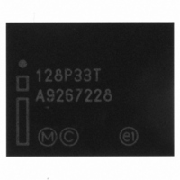
PC28F128P33T85A NUMONYX, PC28F128P33T85A Datasheet - Page 56

PC28F128P33T85A
Manufacturer Part Number
PC28F128P33T85A
Description
IC FLASH 128MBIT 85NS 64EZBGA
Manufacturer
NUMONYX
Series
StrataFlash™r
Datasheet
1.PC28F128P33T85A.pdf
(96 pages)
Specifications of PC28F128P33T85A
Format - Memory
FLASH
Memory Type
FLASH
Memory Size
128M (8Mx16)
Speed
85ns
Interface
Parallel
Voltage - Supply
2.3 V ~ 3.6 V
Operating Temperature
-40°C ~ 85°C
Package / Case
64-TBGA
Cell Type
NOR
Density
128Mb
Access Time (max)
85ns
Interface Type
Parallel/Serial
Boot Type
Top
Address Bus
23b
Operating Supply Voltage (typ)
2.5/3.3V
Operating Temp Range
-40C to 85C
Package Type
EZBGA
Sync/async
Async/Sync
Operating Temperature Classification
Industrial
Operating Supply Voltage (min)
2.3V
Operating Supply Voltage (max)
3.6V
Word Size
16b
Number Of Words
8M
Supply Current
28mA
Mounting
Surface Mount
Pin Count
64
Lead Free Status / RoHS Status
Lead free / RoHS Compliant
Other names
888065
888065
PC28F128P33T85 888065
888065
PC28F128P33T85 888065
Available stocks
Company
Part Number
Manufacturer
Quantity
Price
Company:
Part Number:
PC28F128P33T85A
Manufacturer:
Micron Technology Inc
Quantity:
10 000
11.2.2
11.2.3
Table 30: Device Identifier Information (Sheet 1 of 2)
Datasheet
56
Manufacturer Code
Device ID Code
Block Lock Configuration:
• Block Is Unlocked
• Block Is Locked
• Block Is not Locked-Down
• Block Is Locked-Down
Read Configuration Register
Lock Register 0
To perform an asynchronous page-mode read, an address is driven onto the address
bus, and CE# and ADV# are asserted. WE# and RST# must already have been
deasserted. WAIT is deasserted during asynchronous page mode. ADV# can be driven
high to latch the address, or it must be held low throughout the read cycle. CLK is not
used for asynchronous page-mode reads, and is ignored. If only asynchronous reads
are to be performed, CLK should be tied to a valid V
and ADV# must be tied to ground. Array data is driven onto DQ[15:0] after an initial
access time t
In asynchronous page mode, four data words are “sensed” simultaneously from the
flash memory array and loaded into an internal page buffer. The buffer word
corresponding to the initial address on the Address bus is driven onto DQ[15:0] after
the initial access delay. The lowest two address bits determine which word of the
4-word page is output from the data buffer at any given time.
Synchronous Burst-Mode Read
To perform a synchronous burst-read, an initial address is driven onto the address bus,
and CE# and ADV# are asserted. WE# and RST# must already have been deasserted.
ADV# is asserted, and then deasserted to latch the address. Alternately, ADV# can
remain asserted throughout the burst access, in which case the address is latched on
the next valid CLK edge while ADV# is asserted.
During synchronous array and non-array read modes, the first word is output from the
data buffer on the next valid CLK edge after the initial access latency delay (see
11.1.0.3, “Latency Count” on page
following a minimum delay. However, for a synchronous non-array read, the same word
of data will be output on successive clock edges until the burst length requirements are
satisfied. Refer to the following waveforms for more detailed information:
Read Device Identifier
The Read Device Identifier command instructs the device to output manufacturer code,
device identifier code, block-lock status, protection register data, or configuration
register data (see
issuing the Read Device Identifier command).
on page 56
data values for this device.
•
•
•
Figure 18, “Synchronous Single-Word Array or Non-array Read Timing” on page 34
Figure 19, “Continuous Burst Read, showing an Output Delay Timing” on page 35
Figure 20, “Synchronous Burst-Mode Four-Word Read Timing” on page 35
Item
and
AVQV
Table 31, “Device ID codes” on page 57
delay. (see
Section 9.6, “Device Command Bus Cycles” on page 44
Section 7.0, “AC Characteristics” on page
50). Subsequent data is output on valid CLK edges
BBA + 0x02
Address
0x00
0x01
0x05
0x80
Numonyx™ StrataFlash
Table 30, “Device Identifier Information”
(1)
IH
level, WAIT signal can be floated
show the address offsets and
ID (see
®
Embedded Memory (P33)
RCR Contents
Order Number: 314749-05
DQ0 = 0b0
DQ0 = 0b1
DQ1 = 0b0
DQ1 = 0b1
Lock Bit:
PR-LK0
0089h
Data
Table 31
29).
for details on
November 2007
)
Section


