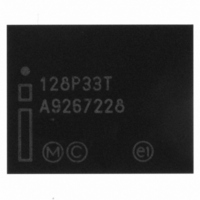
PC28F128P33T85A NUMONYX, PC28F128P33T85A Datasheet - Page 48

PC28F128P33T85A
Manufacturer Part Number
PC28F128P33T85A
Description
IC FLASH 128MBIT 85NS 64EZBGA
Manufacturer
NUMONYX
Series
StrataFlash™r
Datasheet
1.PC28F128P33T85A.pdf
(96 pages)
Specifications of PC28F128P33T85A
Format - Memory
FLASH
Memory Type
FLASH
Memory Size
128M (8Mx16)
Speed
85ns
Interface
Parallel
Voltage - Supply
2.3 V ~ 3.6 V
Operating Temperature
-40°C ~ 85°C
Package / Case
64-TBGA
Cell Type
NOR
Density
128Mb
Access Time (max)
85ns
Interface Type
Parallel/Serial
Boot Type
Top
Address Bus
23b
Operating Supply Voltage (typ)
2.5/3.3V
Operating Temp Range
-40C to 85C
Package Type
EZBGA
Sync/async
Async/Sync
Operating Temperature Classification
Industrial
Operating Supply Voltage (min)
2.3V
Operating Supply Voltage (max)
3.6V
Word Size
16b
Number Of Words
8M
Supply Current
28mA
Mounting
Surface Mount
Pin Count
64
Lead Free Status / RoHS Status
Lead free / RoHS Compliant
Other names
888065
888065
PC28F128P33T85 888065
888065
PC28F128P33T85 888065
Available stocks
Company
Part Number
Manufacturer
Quantity
Price
Company:
Part Number:
PC28F128P33T85A
Manufacturer:
Micron Technology Inc
Quantity:
10 000
11.0
11.1
Table 25: Status Register Description (Sheet 1 of 2)
Datasheet
48
Status Register (SR)
Device Write
Status
DWS
Bit
7
7
6
5
4
3
Device Operations
This section provides an overview of device operations. The system Central Processing
Unit provides control of all in-system read, write, and erase operations of the device via
the system bus. The on-chip WSM manages all block-erase and word-program
algorithms.
Device commands are written to the CUI to control all flash memory device operations.
The CUI does not occupy an addressable memory location; it is the mechanism through
which the flash device is controlled.
Status Register
To read the Status Register, issue the Read Status Register command at any address.
Status Register information is available to which the Read Status Register, Word
Program, or Block Erase command was issued. SRD is automatically made available
following a Word Program, Block Erase, or Block Lock command sequence. Reads from
the device after any of these command sequences outputs the device’s status until
another valid command is written (e.g. the Read Array command).
The Status Register is read using single asynchronous-mode or synchronous burst
mode reads. SRD is output on DQ[7:0], while 0x00 is output on DQ[15:8]. In
asynchronous mode the falling edge of OE#, or CE# (whichever occurs first) updates
and latches the Status Register contents. However, when reading the Status Register in
synchronous burst mode, CE# or ADV# must be toggled to update SRD.
The Device Write Status bit (SR[7]) provides overall status of the device. SR[6:1]
present status and error information about the program, erase, suspend, V
block-locked operations.
Erase Suspend Status (ESS)
Device Write Status (DWS)
Suspend
Status
Erase
Program Status (PS)
ESS
V
6
Erase Status (ES)
PP
Status (VPPS)
Name
Erase Status
ES
5
Program
Status
0 = Device is busy; program or erase cycle in progress; SR[0] valid.
PS
0 = V
1 = Program fail or program sequence error when set with SR[5,7]
4
1 = Erase fail or program sequence error when set with SR[4,7].
PP
1 = V
within acceptable limits during program or erase operation.
V
PP
PP
1 = Device is ready; SR[6:1] are valid.
VPPS
< V
Status
3
0 = Erase suspend not in effect.
Numonyx™ StrataFlash
1 = Erase suspend in effect.
PPLK
0 = Program successful.
0 = Erase successful.
during program or erase operation.
Description
Suspend
Program
Status
PSS
2
Block-Locked
®
Embedded Memory (P33)
Status
Order Number: 314749-05
BLS
1
Default Value = 0x80
November 2007
PP
, and
Status
Write
BEFP
BWS
0


